Design and Implementation of a Real Random Number Generator Based on FPGA
The True Random Number Generator (TRNG) has a wide range of applications in statistics, information security and other fields. In these fields, not only are data sequences evenly distributed and independent of each other, but they are also required to be unpredictable and capable of resisting attacks against randomness. B. Sunar, WJ. MarTIn and D. R. STInson proposed that the performance of a true random number generator is affected by three factors: Entropy Source, Harves TIng Mechanism, and Post-Processing. The three most common methods of generating true random numbers in a circuit system are:
1) Direct amplification method: physical noise such as resistance thermal noise in the amplifying circuit, and a random number sequence is obtained after comparison by a comparator;
2) Oscillation sampling method: using a slow oscillator with jitter to sample a fast oscillator with a fixed period through a D flip-flop, and output a random sequence;
3) Discrete-time chaotic method: The random sequence is generated by the unpredictable chaotic circuit and the dependence on the initial condition.
Based on the structure of the analog circuit, the statistical distribution of the entropy source is more ideal, and the entropy source noise does not change with the change of the sampling period; based on the structure of the digital circuit, the integration is high, and it is easy to implement on a general programmable platform such as FPGA, but the entropy source The statistical characteristics are not ideal compared to analog circuits.
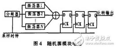
This paper attempts a TRNG structure implemented with pure digital circuits, and does not use special resources such as PLL, which facilitates the design of FPGA migration to chip design. The core idea is to use an inverter and a delay unit to form two independent oscillators. The phase offset due to the difference of internal noise is used as the entropy source. After a period of oscillation, the random state is determined by the digital bistable circuit. Latch. The outputs of multiple sets of oscillators are XORed and synchronized to obtain a random sequence. The TRNG was implemented on the FPGA physical platform and tested and verified.
1 TRNG design 1.1 Phase drift and jitterDue to the influence of noise in the circuit, the period of the clock signal in the digital circuit may be shortened or lengthened at each different cycle, which is clock jitter. Jitter can be measured and characterized in many ways, it is a random variable with a mean of zero. The difference in oscillator start-up time and the process variation of the circuit components cause phase drift between the oscillators. Therefore, the jitter signal and phase shift are suitable as a random source of TRNG in digital circuits.
1.2 metastable stateThe latch is a bistable device with two stable states of logic '1' and '0', but in special cases it may enter a metastable state, where its output is between '1' and '0'. The intermediate level between. The latch shown in Figure 1 is characterized by two inverters and two switches. When the latch is turned on, the sampling switch is closed and the hold switch is turned on (Figure a); when the latch is closed, the sampling switch is turned on and the switch is held closed (Figure b). Figure c shows the DC transfer characteristics of the two inverters. When the latch is off, A=B, the steady state is A=B=0 and A=B=VDD, and the metastable state is A=B=Vm, where Vm is not a reasonable logic value. Since the level is mutually stable at this point and can stay indefinitely, the point is said to be metastable. However, any noise or other interference will cause A and B to eventually stabilize in one of the two steady states. Figure d is a very vivid representation of the metastable state, it is like any interference in the small ball at the top of the mountain will cause the ball to roll to the steady state of the two ends of the mountain.

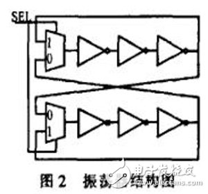
As shown in FIG. 2, the binary multiplexer is used as both a delay unit and a strobe unit. When the strobe signal is '1', two mutually independent, free-running ring oscillators are formed. When the strobe signal is '0', the two sets of inverters are connected across each other to form a bistable device. When free to oscillate, there is jitter and phase shift between the two oscillators. At the moment when the oscillation stops, that is, when the oscillation loop is broken and the two sets of inverters are cross-connected, the absolute sum of the instantaneous output voltage of the inverter and the internal noise determines which logic value the circuit is finally stabilized. Sometimes even if the inverters are connected together, the circuit will oscillate for a long time to stabilize and form a metastable state. In summary, the source of the random sequence uses both jitter and metastable mechanisms.

The waveform is shown in Figure 3. In order to facilitate the data acquisition strobe signal is obtained by dividing the clock by frequency. In the free-running phase, the rapid change of the output signal does not belong to any steady state, and is indicated by a slash in the figure. During the parsing phase, the circuit is a bistable device, and the parsing time should be kept long enough that the output level is stable to logic '1' or '0' in most cases.

The output of each oscillator can be added to the randomness by XOR operation, and the propagation of the metastable state will cause the wrong operation of the subsequent circuit. Therefore, the synchronizer is used to isolate the random sequence after the XOR with the subsequent circuit, and it is also convenient to collect. A stable output sequence for performance analysis. Here, the synchronization structure of the three-level register is adopted. According to the definition of MTBF (Mean TIme Between Failure), it takes an average of hundreds of years for a metastable event to propagate downward through the synchronizer, so the design is satisfied. required. The circuit diagram of this module is shown in Figure 4.

The handheld addresser is used to program the address of the monitoring module offline. When in use, connect the two output wires of the handheld encoder to the communication bus terminal (terminal label 1, 2) of the monitoring module, turn on the black power switch on the right side upwards, and press "ten Add", [Subtract ten", [Add one place" and [Subtract one place" to program the address.
Hd Encoders,Twitch Encoder,Resolver Encoder,Incremental Rotary Encoders
Changchun Guangxing Sensing Technology Co.LTD , https://www.gx-encoder.com