Zener diode working principle and precautions
 The following is the circuit diagram of [Zener diode working principle and precautions]
 Zener diode working principle and precautions
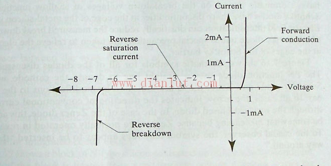
Under normal conditions, there is only a small current in the reverse biased PN junction. This leakage current is kept constant until the reverse voltage exceeds a certain value. After this value, the PN junction suddenly starts to have a large current conduction (Figure 1.15). This sudden and significant reverse conduction is a reverse breakdown, which can cause damage to the device if there are no external measures to limit the current. Reverse breakdown typically sets the maximum operating voltage of the solid state device. However, the reverse breakdown can be used as a very stable reference voltage if appropriate precautions are taken to limit the current. 
Figure 1.15 Reverse breakdown of the PN junction diode.
One mechanism that causes reverse breakdown is avalanche multiplication. Consider a reverse biased PN junction. The depletion region widens as the bias rises, but not fast enough to prevent the electric field from strengthening. A powerful electric field accelerates some carriers through the depletion region at very high speeds. When these carriers collide with atoms in the crystal, they strike loose valence electrons and generate additional carriers. Because a carrier can generate extra thousands of carriers by impact, it is like a snowball can produce an avalanche, so this process is called avalanche multiplication.
Another mechanism for reverse breakdown is tunneling. Tunneling is a quantum mechanism process that enables particles to move a small distance without any obstacles. If the depletion region is thin enough, the carriers can jump over by tunneling. The tunneling current is mainly determined by the width of the depletion region and the voltage difference across the junction. The reverse breakdown caused by Tunneling is called Zener breakdown.
The reverse breakdown voltage of the junction depends on the width of the depletion region. The wider the depletion region, the higher the breakdown voltage is required. As previously discussed, the lighter the doping, the wider the depletion region and the higher the breakdown voltage. When the breakdown voltage is less than 5 volts, the depletion region is too thin, mainly Zener breakdown. When the breakdown voltage is higher than 5 volts, it is mainly avalanche breakdown. The PN diodes designed to work in the reverse-conducting state are called Zener diodes or avalanche diodes according to the dominant working mechanism. The breakdown voltage of the Zener diode is less than 5 volts, while the breakdown voltage of the avalanche diode is higher than 5 volts. Engineers often refer to them as Zener tubes regardless of how they work. Therefore, the 7V Zener tube, which relies mainly on avalanche breakdown work, may be confusing.
In fact, the breakdown voltage of a junction is not only related to its doping characteristics but also to its geometry. The above discussion analyzes a planar junction where two uniformly doped semiconductor regions intersect in one plane. Although some true knots approximate this ideal, most knots are curved. The curvature enhances the electric field and reduces the breakdown voltage. The smaller the radius of curvature, the lower the breakdown voltage. This effect has a large effect on the breakdown voltage of the thin junction. Most Schottky diodes have a distinct fault at the edge of the metal-silicon interface. Electric field enhancement can greatly reduce the measured breakdown voltage of a Schottky diode unless there are special measures to weaken the electric field at the edge of the Schottky barrier.
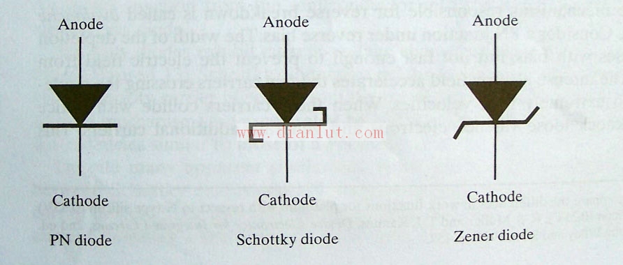
Figure 1.16 is all the circuit symbols discussed above. The PN junction uses a straight line to represent the cathode, while the Schottky diode and Zener diode make some modifications to the cathode end. In all of these legends, the direction of the arrows indicates the direction of the current under forward bias of the diode. In Zener diodes, this arrow can be somewhat misleading because the Zener is normally operating in a reverse biased state. For the casual observer, this symbol should be inserted next to the phrase "the direction is reversed." 
Figure 1.16 Circuit diagram symbols for PN junction, Schottky, and Zener diodes. In some circuit diagram symbols, the arrows are hollow or half arrows.
Zener tubes generally have two uses (the following IZ is the operating current, UZ is the nominal regulated voltage, UW is the actual operating voltage):
1 In normal operation, it is in the "on" state, IZ≥0.1mA level, at this time the Zener tube acts as a voltage regulator, UW≈UZ.
2 "Off" state during normal operation, ie UW
In fact, the commonly used Zener tubes are mainly divided into two categories, one is the so-called "regulator tube" and the other is the TVS type device. The former is usually the first usage, the latter is usually the second usage. But it is not absolute, the two are only characteristic parameters. Ordinary Zener can also be used as a protection device, but the response speed is poor, and it is not suitable for occasions where it is necessary to suppress extremely high-speed pulse interference. TVS can also be used as a regulator, and of course not suitable.
To sum up, I found that beginners often make the following mistakes:
1. Think of the Zener characteristics too good: when UW7V), the curve is still okay, change a low voltage, such as 3V, then the actual curve is really "soft", there is a large current at 1.5V, until IZ Increased to tens of mA, UZ only lazily reached the nominal value, it is a parabola.
2. With the Zener tube for protection, there is a price for not knowing everything in the world. The price here is the leakage current IR (IZ in the "off" state): IR>0; the second does not understand everything in the world, there is room for it, here The room is to ensure the "cutoff" voltage margin UM: UM = UZ-UW > 0 (IR → very small); three do not understand the world is all elastic (concession), the elasticity here is the UW with the conduction state The increment of IZ increase is UP: UP=UW-UZ>0 (IR→large). And even if you leave room and pay the price, you still have to make concessions. To reduce the IR, it is necessary to increase the ΔU, that is, to select the UZ tube, but this will reduce the "strength" of the protection.
3. I don't understand the dynamic internal resistance of the Zener tube dV/dI>0, that is, UZ will increase with IZ. This is not much to say.
4. I don't understand that the response of the Zener tube is relatively sluggish. The UW changes, and the IZ does not change immediately, but there is a delay. There is also a junction capacitance, and the junction capacitance is sometimes quite large. According to the circuit diagram on the textbook, the Zener tube is connected to the op amp feedback arm for limiting, and it is also self-satisfied for the flexible feedback technology of the op amp. But after inputting a square wave of a few MHz, I found that the output is not the same thing, and it is embarrassing.
From these few items, some principles can be summarized:
1. Try to avoid using low pressure Zener tubes.
2. Use Zener to protect UZ, make UWMAX+UM3. The design circuit must have the concept of "dynamic". The circuit is the same as everyone, and all the machines are unresponsive. The only difference is "slower" and "less slow".
4. Remember Murphy's Law: "Those things can be worse if they can be worse."
Small computer system interface (SCSI) is an independent processor standard for system level interfaces between computers and intelligent devices (hard disks, floppy drives, optical drives, printers, scanners, etc.). SCSI is an intelligent universal interface standard.
VHDCI-90°SCSI Section
ShenZhen Antenk Electronics Co,Ltd , http://www.coincellholder.com