Solid state relay and its basic working principle diagram
In order to let everyone better understand the working principle of solid state relays, Xiao Bian specially gave the working principle diagram of solid state relays. Combined with the working principle diagram of solid state relays, it is more convenient and intuitive to explain the working principle of solid state relays. Despite the numerous specifications of solid state relays on the market, the working principle of solid state relays is basically similar. It mainly consists of three parts: input (control) circuit, drive circuit and output (load) circuit. The working principle of the solid state relay is illustrated by the working principle diagram of two solid state relays.
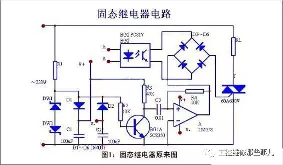
Solid state relay schematic diagram 1:

The topped sinusoidal signal taken from DW1 and DW2 is outputted by the inverter BG1 and then output by the operational amplifier A to output a spike signal. The spike is applied between the AC diagonal of D3~D6 and the control pole and cathode of the SCR. The DC diagonal of D3~D6 is connected to the output of the optocoupler. When a low-voltage small-current signal is input from A and B, the diode emits light, and the photosensitive tube is turned on, so that the spike outputted from the A operational amplifier triggers the SCR to be turned on, and the angular load RL is energized. When A and B have no signal input, the photocoupler BG2 is turned off, and the spike is not passed, so that the SCR cannot be turned on.
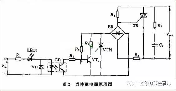
Solid state relay schematic diagram 2:

When there is no input signal, the phototransistor in GD is cut off. VT1 is the AC voltage zero detector. The base current is obtained by R3 and satisfies the conduction. The gate of VTH is clamped to the low potential and is turned off. When there is an input signal, the phototransistor is turned on. At this time, the state of VTH is determined by VT1. When the power supply voltage is greater than the zero-crossing voltage, the voltage of the voltage divider P of the voltage divider R3 and R2 is greater than VBE1, and the VT1 is saturated. The SCR gate is turned off due to the clamp being at a low potential, and the gate of the TR is turned off due to the absence of a trigger pulse. Only when the power supply voltage is less than the zero-crossing voltage, when the voltage at point P is less than VBE1, G1 is turned off, and the SCR gate is turned on by the trigger signal. The trigger pulse is obtained at the gate of the TR, and the TR is turned on. Thereby the load power is turned on.

Rf Duplexer,Coaxial Duplexer,Microwave Duplexer,Diplexer And Duplexer
Chengdu Zysen Technology Co., Ltd. , https://www.zysenmw.com