Talking about the Complexity and Uncertainty of Parasitic Extraction of Fin Field Effect Transistor (finFET)
The introduction of fin field effect transistors (finFETs for short) marks the first time CMOS transistors are considered true three-dimensional devices. Complexity and uncertainty are caused by the source-drain regions and the three-dimensional structure of the connections to them, including local interconnects and contact vias.
As a result, device modeling has to be improved quickly. The BSIM Group of UC Berkeley Device Group has developed a model called BSIM-CMG (Universal Multi-Gate) to represent the resistors and capacitors present inside the finFET. To help alleviate concerns about the transition to the finFET process, fabs have made great efforts to provide device and parasitic accuracy data, as well as to preserve usage models for previous processes.
Although we have BSIM-CMG as a general way of representing finFET design parameters, each fab will increase or decrease the components of the standard model to more accurately represent the parasitic effects around it. This customization has been driven by a number of initiatives, including wafer fabs using their own device and parasitic parametric models to match silicon verification results, and electronic design automation (EDA) tools to predict results on silicon.
In addition, at advanced process nodes, fabs want their processes, they use scientific field solvers to create "gold (1340.40, -1.60, -0.12%)" models for these processes, and EDA vendors develop And there is a closer relationship between the output of the extraction tool used by the designer in the field. At the 28-nm node, fabs expect the error rate of commercial extraction tools to remain within 5-10% of the standard model. For the finFET process, the fab requires an average accuracy error of less than 2% of the standard model and a three-sigma standard deviation of only 6-7%.
Due to the complexity of the FinFET interaction, a 3D field solver is essential to meet the fab's requirements for EDA vendors' parasitic extraction tools and fab standard model results. For the first time, designers will be able to see the field solver results, which have so far been used primarily for process characterization rather than design. Fortunately, this usage model does not change during parasitic extraction because these tools will automatically switch between the field solver and the heuristic.
Traditionally, field solvers are not practical for production because they require too much computation time (that is, too slow). At Mentor, we developed the Calibre "xACT3D" extraction tool to solve this problem. With adaptive mesh technology to speed up calculations, the tool is an order of magnitude faster or more. It also has an extensible architecture that leverages multiple CPUs in a modern computing environment. Therefore, it is easy to design a field solver calculation scheme for a layout on a 32-bit CPU machine. These layouts include small to small cells and large to millions. Large module of transistors.
However, for a full chip, we need to handle the design of billions of transistors, including tens of millions of wires on the top. From a turnaround time perspective, it is impractical to use only a fast field solver. We need smart techniques and heuristics, first using field solver techniques for complex structures, and then using lookup tables for common geometry. It is possible to convert the windings in the high level to the lookup table method because the electric field modeling in the routing grid is similar to that seen in the previous nodes. In fact, the first generation of finFET devices used the 20nm interconnect method used by fabs in planar processes.

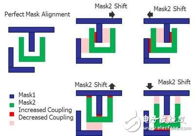
Figure 1: The possible misalignment of the dual imaging (DP) reticle requires the designer to evaluate more corns for parasitic extraction to verify the timing and performance of the integrated circuit.
When considering top-level interconnect extraction, we need a more efficient calculation method because the parasitic parameters that must be calculated increase. In addition, as dual imaging (DP) and multiple imaging (MP) play an increasingly important role in manufacturing (starting at 20 nanometer nodes), the number of interconnected corners will also increase significantly. At the 28 nm node, there may be 5 interconnected corners, but at the 16 nm node we will see 11 to 15 corners. A traditional approach to increasing computing requirements is to use more CPUs and increase the scalability of computer core operations. We are doing this, but we are still implementing advanced mulTI-corner analysis techniques to achieve more efficient calculations. In the past, we estimated that for each additional corner, the runtime would be doubled (compared to a single corner). Now, we can process multiple corners in parallel, increasing the overall turnaround time by only 10% for each additional corner. This means that 15 corners now require 2.5 times longer runtime than a single corner. By using advanced mulTI-corner analysis and leveraging more CPU balance, we can make designers' turnaround times as short or as short as 28nm or 20nm.
The recent rapid transition to the finFET process has created challenges for the EDA industry, requiring the industry to quickly come up with effective solutions to complex new problems. There is more work to be done, but it can be said that compared to the same stage in the development of the previous process node, we now have a comparison between the EDA tool on the finFET process and the silicon verification of the fab. data.
Jumei Video(Shenzhen)Co.,Ltd , https://www.jmsxdisplay.com