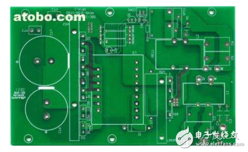
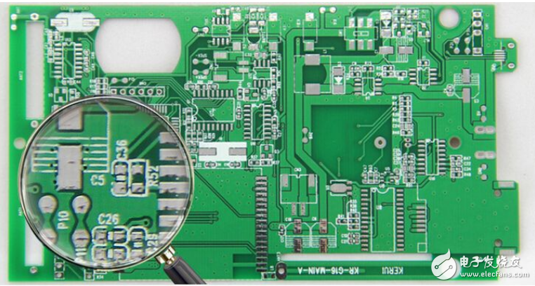
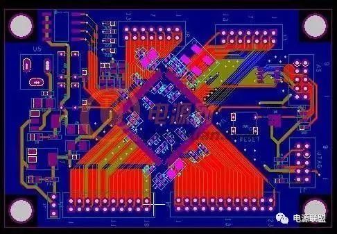
Method and precautions for reducing electromagnetic interference of PCB design
Electromagnetic compatibility design is closely related to the specific circuit. In order to design the electromagnetic compatibility, the designer needs to minimize the radiation (the RF energy leaking from the product) and enhance its radiation (the energy entering the product). Susceptibility and anti-interference ability. For the common conduction coupling at low frequencies, the common radiation coupling at high frequencies, cutting off the coupling path must be given full attention in design. This article mainly explains the places to pay attention to when designing PCBs, thus reducing the electromagnetic interference problem in PCB boards.
PCB design principlesAs the board integration and signal frequency are getting higher and higher with the development of electronic technology, it is inevitable to bring electromagnetic interference. Therefore, the following principles should be followed when designing the PCB, so that the electromagnetic interference of the board is controlled within a certain range. , to meet design requirements and standards, improve the overall performance of the circuit.
1. Selection of circuit board
The primary task of PCB design is to properly select the size of the board. If the size is too large, the impedance between the components will be too long, and the impedance of the line will increase, and the anti-interference ability will decrease. The arrangement is dense, which is not conducive to heat dissipation, and the connection is too fine and too dense, which is easy to cause crosstalk. Therefore, the appropriate size of the board should be selected according to the components required by the system.

The board is divided into single, double and multi-layer boards. The selection of the number of layers of the board depends on the function to be implemented by the circuit, the noise figure, the number of signals and the number of network lines. A reasonable number of layers can reduce the electromagnetic compatibility of the circuit itself. The general selection principle is: 1 for the signal frequency is medium and low frequency, fewer components, the wiring density is lower or medium, select single panel or double panel; 2 for high wiring density, high integration and more components Multi-layer board; 3 for high-frequency, high-speed integrated circuits, densely-selected 4 layers or more layers of boards. The multilayer board can be designed as a separate power layer, signal layer and ground plane. The signal loop area is reduced, and the differential mode radiation is reduced. For this reason, the multilayer board can reduce the radiation of the circuit board and improve the anti-interference ability.
2. Layout of circuit board components
After determining the PCB size, the position of the special component should be determined. Finally, according to the functional unit of the circuit, all the components of the circuit are arranged in blocks. The digital circuit unit, the analog circuit unit and the power supply circuit unit should be separated, and the high frequency circuit unit and the low frequency circuit unit should also be separated. The layout principles of common boards are as follows.
1) The principle of determining the location of a particular component:
1 heating elements should be placed in a position to facilitate heat dissipation, such as the edge of the PCB, and away from the microprocessor chip; 2 special high-frequency components should be placed next to each other to shorten the connection between them; 3 sensitive components should be away from the clock Generator, oscillator and other noise sources; 4 potentiometers, adjustable inductors, variable capacitors, pushbutton switches and other adjustable components should be arranged in line with the structural requirements of the machine, easy to adjust; 5 heavy mass components should be bracketed Fixed; 6 EMI filter should be placed close to the EMI source.
2) According to the circuit function unit, the principle of layout of the umbrella components of the circuit:
1 Each functional circuit should determine the corresponding position according to the signal flow direction between them, which is convenient for wiring;
2 Each functional circuit should first determine the position of the core components, and place other components around the core components to minimize the connection between components;
3 pairs of high frequency circuits, should consider the distribution parameters between components;
4 components placed on the edge of the board should be no less than 2mm from the edge of the board;
5DC/DC converters, switching tubes and rectifiers should be placed as close as possible to the transformer to reduce external radiation;
6 Voltage regulator components and filter capacitors should be placed close to the rectifier diode.
3) Power and ground wiring principles
Whether the PCB's power and ground wiring is reasonable is the key to reducing electromagnetic interference throughout the board. The design of power and ground lines is a problem that cannot be ignored in PCBs. It is often the most difficult design. The following principles should be followed in design.

1) Power and ground wiring skills
The wiring on the PCB is characterized by distributed parameters such as impedance, capacitive reactance, and inductive reactance. In order to reduce the influence of PCB layout parameters on high-speed electronic systems, the principle of power and ground wiring is:
1 increase the spacing of the traces to reduce crosstalk of capacitive coupling;
2 The power and ground lines should be paralleled to achieve the best distributed capacitance;
3 According to the magnitude of the carrying current, the width of the power line and the ground line should be increased as much as possible to reduce the loop resistance, and the direction of the power line and the ground line in each functional circuit and the direction of signal transmission are the same, which helps to improve Anti-interference ability;
4 The power supply and ground should be directly routed on the top of each other, so as to reduce the inductance and minimize the loop area, try to make the ground wire under the power line;
5 The thicker the ground wire, the better, the width of the general ground wire is not less than 3mm;
6 The ground line constitutes a closed loop to reduce the potential difference on the ground line to improve the anti-interference ability;
7 In the design of multi-layer board wiring, one layer can be regarded as “all-ground planeâ€, which can reduce the grounding impedance and at the same time shield.
2) Grounding skills of each functional circuit
The grounding methods of each functional circuit of the PCB are divided into single-point grounding and multi-point grounding. Single-point grounding is divided into single-point series grounding and single-point parallel grounding according to the connection form, as shown in Figure 3 and Figure 4. Single-point series grounding Due to the different lengths of the grounding conductors, the grounding impedance of each circuit is different, and the electromagnetic compatibility is reduced, which is often used for protective grounding. Single-point parallel connection Each circuit has its own grounding wire, so the mutual interference is small, but the grounding wire may be extended and the grounding impedance may be increased. It is often used for signal grounding, analog grounding, and power grounding. Multi-point grounding means that each circuit has a grounding point, as shown in Figure 5. Multi-point grounding is commonly used in high-frequency circuits, with a short grounding wire and a small grounding impedance, reducing the interference of high-frequency signals.
In order to reduce the interference caused by grounding, the grounding must also meet certain requirements:
1 The grounding wire should be as short as possible, and the grounding surface should be large;
2 Avoid unnecessary ground loops and reduce the interference voltage of the common ground;
3 The grounding principle is to adopt different grounding methods for different signals, and it is not possible to take the same grounding point for all grounding;
4 When designing a multi-layer PCB, the power layer and the ground layer should be placed in adjacent layers as much as possible so that the capacitance of the layer is formed in the circuit to reduce electromagnetic interference;
5 Try to avoid strong and weak signals, digital and analog signals.

24 tips to reduce noise and electromagnetic interference
(1) High-speed chips can be used in key places without using high-speed chips.
(2) The resistance of the upper and lower edges of the control circuit can be reduced by using a string of resistors.
(3) Try to provide some form of damping for relays, etc.
(4) Use the lowest frequency clock that meets the system requirements.
(5) The clock generator is as close as possible to the device using the clock. The quartz crystal oscillator housing should be grounded.
(6) Circle the clock area with the ground wire and keep the clock line as short as possible.
(7) The I/O drive circuit should be as close as possible to the side of the printed board, allowing it to leave the printed board as soon as possible. The signal entering the printed board should be filtered, and the signal from the high-noise area should be filtered. At the same time, the signal of the string termination is used to reduce the signal reflection.
(8) The useless end of the MCD should be connected high, or grounded, or defined as an output. The end of the integrated circuit should be connected to the power supply ground. Do not hang it.
(9) Do not leave the input terminal of the unused circuit, the unused input terminal is grounded, and the negative input is connected to the output.
(10) As far as possible, the printed board should use 45 fold lines instead of 90 fold lines to reduce the external transmission and coupling of high frequency signals.
(11) The printed board is divided according to the frequency and current switching characteristics, and the noise component is farther away from the non-noise component.
(12) Single-panel and double-panel single-point power supply and single-point grounding, power supply line and grounding wire are as thick as possible. If the economy is affordable, use a multi-layer board to reduce the power supply and grounding inductance.
(13) Keep the clock, bus, and chip select signals away from the I/O lines and connectors.
(14) The analog voltage input line and reference voltage terminal should be as far as possible from the digital circuit signal line, especially the clock.
(15) For A/D type devices, the digital part and the analog part are more uniform and do not cross.
(16) The clock line is perpendicular to the I/O line and has less interference than the parallel I/O line. The clock component pins are far from the I/O cable.
(17) The component pins are as short as possible, and the decoupling capacitor pins are as short as possible.
(18) The key lines should be as thick as possible and with protective ground on both sides. The high speed line should be short and straight.
(19) Noise-sensitive lines should not be parallel to high current, high-speed switching lines.
(20) Do not route underneath the quartz crystal and below the noise sensitive device.
(21) Weak signal circuit, do not form a current loop around the low frequency circuit.
(22) Do not form a loop in the signal. If it is unavoidable, make the loop area as small as possible.
(23) One decoupling capacitor per integrated circuit. A small high frequency bypass capacitor is added to each electrolytic capacitor.
(24) Use a large-capacity tantalum capacitor or a condenser capacitor instead of an electrolytic capacitor for the circuit to charge and discharge the storage capacitor. When using a tubular capacitor, the housing should be grounded.
Iron Case Junction Box Led Driver
With the North American Canadian market on the safety level requirements are too high, the wiring can not be exposed, so now produce some iron box shell packaging power supply for panel lights, troffer, can also be used for industrial electricity, 100 -347V input. Waterproof level is low, so for indoor dry environment.
Surface Mounted Led Panel Light,Led Panel Light 60W Driver,Ul Dimmable Transformer
ShenZhen Fahold Electronic Limited , https://www.fahold.net