What are the main functions of the latch?
The so-called latch is that the state of the output does not change with the state of the input. Only when there is a latch signal, the state of the input is saved to the output until the next latch signal arrives. A typical latch logic circuit is a D flip-flop circuit. PS: Latch signal (that is, the input signal of the Data terminal when LE is assigned to a high level). Latching is to temporarily store the signal to maintain a certain level state.
The main role of the latch1: cache,
2: Complete high-speed control of its out-of-synchronization problems with slow peripherals,
3: It is to solve the problem of driving (the current supplied is larger than the output current of 51IO port)
4: Expand the I / O port (can be very cumbersome to use the latch power superposition method, that is, the Q of the latch is connected to the latch ~ to achieve unlimited expansion of the IO port ···)
Latch application example:I/O port multiplexing: When the MCU is connected to the off-chip memory, the latch is connected. This is to achieve address multiplexing. Assume that the eight I/O pins of the MCU port are used for both the address signal and the data signal. In this case, the latch can be used to latch the address first. (Specific operation: first send the address information, the ALE enable latch will latch the address information at the address end of the peripheral, and then send the data information and the read/write enable signal to read and write at the specified address)
If the bus interface of the microcontroller is only used for one purpose, there is no need to connect the latch; if the bus interface of the microcontroller is to be used for two purposes, the latch is used. For example, an I/O port needs to control two LEDs. When data is sent to the first LED, the first latch is "opened" and the second latch is "locked" to the second LED. The data is unchanged. When data is sent to the second LED, the second latch is "opened" and the first latch is "locked" so that the data on the first LED does not change. If one port of the microcontroller is to be used for three purposes, three latches can be used, and the operation process is similar. For this usage, the latch can be thought of as an expander for the I/O port of the microcontroller.
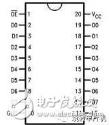
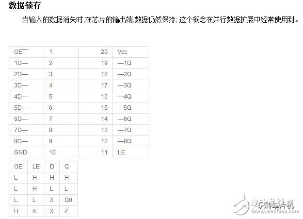
74HC573 pin distribution diagram

It can be seen from the truth table above: When OE is high, the output is always in a high-impedance state. At this time, the chip is in an uncontrollable state, so in general applications, we must connect OE to a low level.
LE is the output state change enable. When LE is low, the output Q always keeps the last stored signal (input from D). When LE is high, Q follows the state of D. And latch the state of D.
That is to say, when the latch enable LE is high, the latches of these devices are transparent to the data (that is, the output is synchronized). When the latch enable goes low, data that matches the setup and hold times is latched.
In addition: the inputs to the latches are compatible with standard CMOS outputs; if added with pull-up resistors , they are compatible with LS/ALSTTL outputs.
Detailed description of the circuit connection and use of the latch:(in combination with the above latch pin description)
0: vcc gnd Power supply needless to say?
1: OE ground
2: D0-D7 is connected to our signal transmitter (usually the I/O port used by the MCU to transmit data)
3: Q0-Q7 connects to the terminal we want to receive information (digital tube, LCD, or anyother device)
4: LE is connected to an I/O port (this I/O pin can be regarded as a switch for the latch latch function, and the high level is to update the Q terminal signal (the signal to be updated is input from D). The low level is not updated. )
Shenzhen Happybate Trading Co.,LTD , https://www.happybateprojectors.com