AD9234 Reference Design Circuit | Analog to Digital Converter Application Circuit
The AD9234 is a dual, 12-bit, 1 GSPS/500 MSPS ADC. The device features an on-chip buffer and sample-and-hold circuitry designed for low power, small size, and ease of use. This product is used to sample wide bandwidth analog signals. The AD9234 is optimized for wide input bandwidth, high sample rate, excellent linearity, and low power consumption in a small package.
This dual ADC core features a multi-stage, differential pipeline architecture with integrated output error correction logic. Each ADC has a wide bandwidth buffer input that supports a variety of user selectable input ranges. An integrated voltage reference simplifies the design. The data output of each ADC is internally connected to an optional divide-by-2 clock. The AD9234 has several built-in features that simplify the automatic gain control (AGC) function in communication receivers.
AD9234 product features:
1. Low-power analog core, 12-bit, 1.0 GSPS dual-channel analog-to-digital converter (ADC), 1.5 W per channel.
2. Wide full power bandwidth, supporting IF signal sampling up to 2 GHz.
3. Providing a buffered input to the programmable input simplifies filter design and implementation.
4. Flexible Serial Port Interface (SPI) controls various product features and functions to meet specific system requirements.
5, programmable fast overrange detection.
AD9234 application:
1, communication
2, diversity multi-band, multi-mode digital receiver
3, 3G/4G, TD-SCDMA, W-CDMA, GSM, LTE
4. Point-to-point radio system
5, digital predistortion observation path
6, instrumentation (spectrum analyzer, network analyzer, integrated RF test solution)
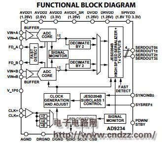
Internal function diagram of AD9234:

Figure 1: Internal Functional Diagram of the AD9234
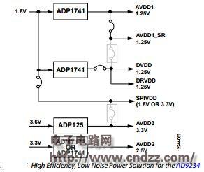
AD9234 High Efficiency, Low Noise Power Solution:

Figure 2: AD9234 High Efficiency, Low Noise Power Solution
The AD9234 must be equipped with the following seven items: AVDD1 = 1.25 V, AVDD2 = 2.5 V, AVDD3 = 3.3 V, AVDD1_SR = 1.25 V, DVDD = 1.25 V, DRVDD = 1.25 V, and SPIVDD = 1.8 V. The need for the best the application of high power efficiency and low noise performance, the recommended ADP2164 and ADP2370 switching regulator for converting the 3.3 V, 5.0 V, or 12 V input rail to the middle rail (1.8 V and 3.8 V). These intermediate tracks are then adjusted by very second low noise, low dropout (LDO) regulators (ADP1741, ADM7172, and ADP125). Figure 2 shows the recommended power supply for the AD9234.
AD9234 Datasheet: Download Now
More schematics and PCB code:
Twinkle System Technology Co Ltd , https://www.pickingbylight.com