LCD split screen and cut screen principle analysis, segmented LCD screen design principle
In fact, the relationship between the driving waveform and the liquid crystal display is very simple. Just remember that the liquid crystal cannot be added with DC power, and which waveforms are all used to make an AC driving voltage signal. Although the waveforms of COM and SEG seem complicated, in fact, it is very simple, COM is a sequence. Scanning the pulse sequence, the appearance of the recurrence, can be lit up, just look at the pressure difference relationship between the COM and SEG waveforms.
For example, the driver chip COM and SEG of 3V 1/2bias should illuminate the liquid crystal. Only when COM is 3V SEG is 0V or COM is 0V SEG is 3V, and other conditions are not bright.
Bias refers to the bias coefficient of the liquid crystal, which simply indicates the number of steps of the driving voltage. 3v 1/2bias has three voltages 3v 1.5v 0v, ​​3v 1/3bias has four voltages 3v 2v 1v 0v, ​​but all are 3v liquid crystal blocks. Light up, now know what 1/2bias and 1/3bias can calculate. The more the number of bias, the difference between bright and non-bright is obvious, and the contrast is improved.

The specific information in this area is not too much. In fact, it is the fastest way to look at the specifications of different LCD driver chips. There is something that can search some basic principles of liquid crystal on the Internet, but there are few ordinary black and white, but STN, TFT.
How to perform LCD split screen and cut screen? 1.LCM's Fmark functionWhen the R61509V LCM driver chip was recently debugged, there was a problem of a tearing effect (TE) in the solid color test screen. The root cause is that the speed at which the master writes image data is inconsistent with the speed of the LCM brush screen, specifically, the screen speed is faster than the master write speed. Fortunately, many LCM driver chips have a Fmark pin for synchronizing with the master. When Fmark sends a signal to the master, the master starts writing a frame of data, thus ensuring synchronization on both sides. First describe several concepts before telling:

The screen rate is the speed at which the LCM is refreshed. This value is usually set in the initialization CODE of the LCM. For Renesas' R61509V LCD driver, setting the 0x0010 register is to set the screen speed. According to the formula: frame rate = 678KHZ / {(RTN) * DIV * (432 + 8 + 8)}, where 678K is the internal clock source of LCM, RTN is the number of clocks per line, DIV is the division factor, (432+ 8+8) is the line pixel. The measured results are:
0X011F 20HZ, minimum frequency.
0X011A 29HZ
0X0115 36HZ
0X0110 52HZ
0X001C 60HZ
0X0018 70HZ
0X0014 80HZ
If the screen rate is too low, the flicker phenomenon will occur, so it is generally set at 60HZ or higher.
(2) Master write speed WR and chip select CSThese two PIN pins are available for each DBI's LCM, and the operating frequency of the two is the same. Each time the master writes one frame of data, there will be a chip select signal and a corresponding write valid signal of WR. The change of the write frequency of the master is determined by the working state. For example, when shooting, the display writing speed of the shooting dynamic object is faster than the display writing speed of the shooting static object.
If the screen of the screen is not updated, it will update the lcd for 70ms. If the screen is moving, it will be screened for up to 33ms. This means that the CS frequency can only be limited between 1/70 and 1/30, 14.28HZ to 33.33HZ. The highest frequency is already faster than the frame rate of PAL or NTSC, which can ensure that the camera does not lose frame when working or playing video.
(3) Fmark functionTo enable fmark, first ensure that the fmark pin of the master is properly connected to the fmark pin of the LCM; secondly, enable the fmark function of the screen in the LCM initialization to ensure that the LCM periodically sends a signal to the master, and at the same time enables the master. Control the fmark function to ensure that the master receives a fmark signal before writing a frame of data.
LCM fmark has two parameters to configure: First, how many times the screen sends a fmark signal, such as not necessarily every time the screen is sent fmark signal, you can brush a few times to send a fmark signal; second is the position parameter of fmark It can make fmark delay several lines of output, the purpose is to let the master write data to GRAM later, avoiding TE.
Example: There is a case where the IC outputs a te signal after reading the last line from the GRAM, at which time BB starts writing GRAM. But there may be a line of time, the IC starts to read data from the first line of GRAM, and the speed of writing GRAM is slower than the speed of IC reading GRAM. At this time, it may not start writing. Causes reading GRAM over write GRAM, so it will produce tearing on top. To avoid the TE output too early, the write GRAM starts first, so add a delay to ensure that writing GRAM starts after reading the old data.

The root cause of the TE phenomenon is that the speeds on both sides are inconsistent. Specifically, the refresh rate of the LCM is faster than the speed of the data sent by the master. The speed of the two must meet a certain range. As long as the CS period is guaranteed to be between two TE cycles, that is, the CS write frequency cannot be lower than one-half of the TE read frequency, the fundamental condition for the occurrence of the tearing is that the read and write have a crossover. Usually, the Gram speed (WR) is slower than the lcd screen speed (TE) [x2]. As long as the position of the screen is not more than the position of the Gram, there will be no screen cut.
For example, if CS is almost smaller than two TE cycles, you need to brush two data. First, the first screen starts to be swiped, indicating that reading GRAM starts, it is faster, it reads old. Data; immediately after the master starts writing GRAM, about half of the GRAM is written, this time has already finished brushing, and then starts to brush the second one, that is, read and brush from the top of GRAM, read at this time What comes out is the new data just written. Before writing GRAM, the steps of reading can never keep up with the steps written, and there will be no tearing.
If CS is larger than two TE cycles, assuming three equivalents of TE cycles, then only the third TE read cycle, the displayed data is the data of the written GRAM; the first TE reads the old one. Data, the second TE cycle has not been written due to GRAM, but the read step catches up with the GRAM step, resulting in the explicit part of the old part being new, so TE appears. This is the essence.
(5) TE typeWhen the TE display is enabled, you must ensure that both the LCD TE enable of the CPU and the TE function of the LCM drive are turned on. There are two types of TM enable for LCM: VSYSC, VSYNC&HSYNC. The illustration is as follows:
Summary of 2 menote:
As VSYNC of the frame sync signal, each time a pulse is sent, it means that a new one-screen image data starts to be transmitted. As HSYNC of the line sync signal, every time a pulse is sent, it indicates that a new line of image data starts to be sent.
FTTH Fiber Optical Fast Connectors
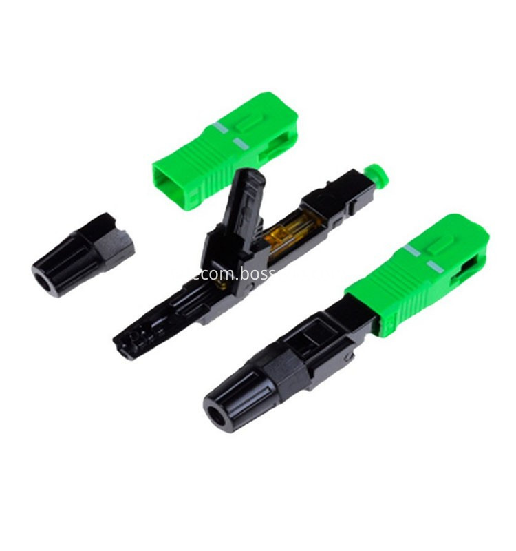
Fiber optic fast connector designed for FTTH. It is a new generation of fiber connector used in assembly. It can provide open flow and precast type, which optical and mechanical specification meets the standard optical fiber connector. It is designed for high quality and high eddiciency for installation, the structure of crimping position is a unique design. The hotest products are SC/APC Fast Connectors and SC/UPC Fast Connectors.

FTTH Fiber Optical Fast Connectors,FTTH SC/UPC Fast Connectors,SC/APC Fast Connectors,LC/APC SM Fast Connectors
NINGBO YULIANG TELECOM MUNICATIONS EQUIPMENT CO.,LTD. , https://www.yltelecom.com