Using Active Bias to Improve Stereo Performance
Using Active Bias to Improve Stereo Performance
| Abstract: This application note discusses the trade-off between active and passive bias circuits in consumer audio products, and compares the use of these circuits in digital potentiometers and volume control. It provides isolation and mute. And other parameters. The formulas provided in this article help designers to evaluate compromised designs in specific situations. |
In this application note, we will compare active and passive bias circuits for digital potentiometers and analyze possible factors that affect device performance. This article also provides designers with formulas to evaluate the design of consumer products in order to properly compromise the design.
Volume control and digital potentiometer The following circuit introduces some terminology used in this article. We will focus on the single power supply situation, because batteries or wall adapter power supply products are very common. In single-supply applications, all circuits are powered by VDD, and the signal swing is between VDD and ground potential. For cost and performance considerations, capacitors may be used between stages or removed.
The wiper buffer can reduce the current through the switch array and improve distortion performance. This article discusses the effect of bias circuits on circuit performance.
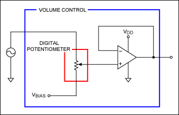
Figure 1. Volume control driven by a signal source
The digital potentiometer (red box part) can be regarded as a switch array and a resistor controlled by a logic circuit, simulating the sliding contact end of a mechanical potentiometer. The volume control IC (blue frame part) is different from the digital potentiometer. It also includes two key circuits required to obtain the best sound quality: the wiper buffer (op amp) and the bias circuit (VBIAS voltage source).
If the passive bias circuit uses a digital potentiometer and requires strict cost control, a passive resistor divider can be used to generate the bias voltage, as shown in Figure 2. The resistance value is generally equal to the value that sets VBIAS at the midpoint of VDD and ground potential. In order to reduce the AC impedance of VBIAS and eliminate noise, most meter personnel will add a bypass capacitor C2.
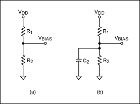
Figure 2. Passive bias circuit
Below the mono volume control circuit, let's examine the influence of the choice of circuit components on the audio performance. Calculate the source impedance of the bias circuit (sometimes referred to as the "stability" of the power supply) from Figure 3.
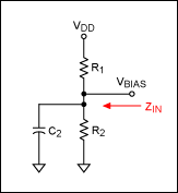
Figure 3. Stability is related to the equivalent impedance of the bias network

First, consider the DC condition (s = 0). The above formula is simplified to the parallel value of resistors R1 and R2, and this resistance value is brought into the volume control circuit (Figure 4).
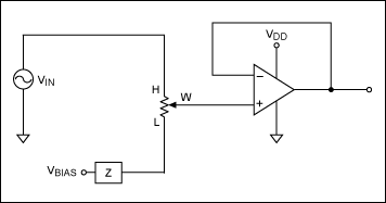
Figure 4. Using a limited impedance bias network to adjust the volume
The finite source impedance of the bias network allows the signal to be applied to the L terminal of the digital potentiometer. Adjusting the sliding end to the L end corresponds to the mute state of the device. Unlike the required no-signal input, the divided signal of the voltage source VIN can be detected here.
For example, if the sliding terminal is at the L terminal, the potentiometer resistance is 40kΩ, and two 10kΩ bias resistors are used, the detected output voltage is:

Under DC conditions, the output is only -19dB lower than the full-scale (dBFS) signal, indicating that even if the potentiometer is set to mute, there is still an output signal.
What effect will it have on the circuit after adding C2? Let's first understand the situation of using 0.01µF capacitor. According to formula 1, the result shown in Fig. 5 is obtained.
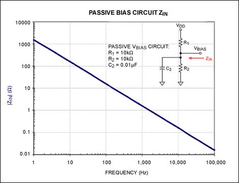
Figure 5. Passive bias network when using a 0.01µF capacitor
After adding C2, it has almost no effect on signals below 1kHz. At 20kHz, the resistance is only reduced to 785Ω, and a silent attenuation of -34dB can be obtained, as shown in Figure 5. The capacitance can be increased to 10µF (or greater) to improve the circuit. At this time, a mute attenuation of -48dB can be obtained at 100Hz, see Figure 6. This is far from the final required volume control performance, and even the audio index under silent conditions cannot be controlled within a reasonable range.
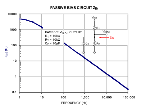
Figure 6. Passive bias network when using 10µF capacitor
Other problems Although we are analyzing the circuit conditions under silent conditions (sliding end is at L), it is obvious that the limited VBIAS impedance will affect all potentiometer settings, and its impact is becoming more and more inaccurate when approaching the low end Decay curve.
How to solve this problem? Then, how to reduce the impedance to make the mute index reach 90dB or better? In order to achieve 90dB, we must control the impedance within the range of single-digit ohms.
The problem caused by reducing R1 and R2 is the increase of DC current, which is not acceptable in practical applications. Obviously, we need to choose C2 to obtain a very low impedance before the frequency reaches the audio frequency band. When choosing a capacitor, it is easy to find that a capacitor that meets the 95dB attenuation requirement at 100Hz cannot be found. For 10kΩ, 10kΩ resistance and 100µF large capacitance, the corresponding attenuation curve is shown in Figure 7. In the discussion of the rest of this article, you will find that a practical solution is to use an active bias circuit.
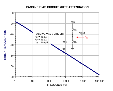
Figure 7. Passive bias network when using 100µF capacitor
Stereo circuit Before discussing the active bias circuit, we first understand the problem of stereo design. For stereo signals, the left and right channels share a passive bias generator, which will cause mute or feedthrough problems. Another problem is crosstalk. Crosstalk refers to a signal leaking from the left (L) channel to the right (R) channel, and vice versa. The reasons for crosstalk are explained below. When the bias circuit is shared between the L channel and the R channel, the circuit is shown in FIG. 8.
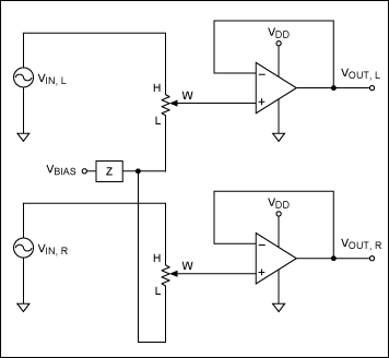
Figure 8. Passive bias network and stereo signal
When the input signal is connected to the H terminal, the limited offset impedance will generate a signal voltage at the L terminal of the digital potentiometer. At this time, the left and right channels share the same bias circuit; therefore, we will get the signal corresponding to the left or right channel VIN at the two VOUT pins. The signal of the input channel has poor mute attenuation or cannot meet the effects of attenuation characteristics. The signal from one channel will appear on the other channel as crosstalk or stereo isolation loss.
Active bias can effectively solve the above problems: provide a very stable or low resistance VBIAS bias source, a typical circuit shown in Figure 9. The divided VDD is buffered by the operational amplifier, and the closed-loop output impedance of the op amp is a few ohms at zero. With the careful design of this circuit, it can reach the 90dB mute suppression index.
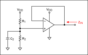
Figure 9. Operational amplifier buffer bias voltage divider
The measurement results compare the operation of the active and passive bias circuits with the test board. Figures 10 and 11 show the typical operating characteristics of the passive and active circuits based on the MAX5457 test board. The passive circuit consists of two 1kΩ resistors and a 4.7µF bypass capacitor. The result is a pole at 68Hz (calculated value) and a continuous sink current of 2.5mA at a 5V power supply.
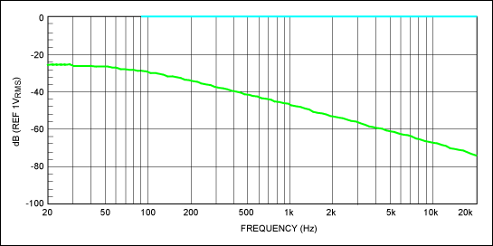
Figure 10. Full-scale and silent response of a digital potentiometer with passive bias
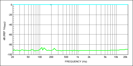
Figure 11. Full-scale and silent response of the digital potentiometer with active bias
With in-phase buffers, active circuits can provide very high resistance. In this case, the bias network can use two 100kΩ resistors without affecting the active bias characteristic curve, and the continuous current consumption is only 25µA.
A better solution—integration! As mentioned above, the performance of passive circuits is very poor, increasing both cost and size. The buffered resistor divider active circuit has better working performance. Of course, this solution increases the overhead of the operational amplifier. So, is it possible to obtain a small size and high-performance solution? The answer is yes, as shown in Figure 12, the volume control IC MAX5486, the above-mentioned functions and digital potentiometers are integrated on a single chip.
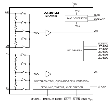
Figure 12. The MAX5486 volume control IC contains VBIAS and wiper buffers for audio applications
Maxim volume control IC series products can be directly connected to microprocessors, buttons, rotary encoders, and even infrared remote controls. Its additional functions, such as: zero-crossing synchronous sliding end control, make this series of ICs very suitable for audio applications.
Military battery has a wide application on some high-tech euquipment including military communications equipment, submarine, drone , warship, government and so on .
The design for Military Battery Pack is more strict than normal lithium or Lipo Battery packs ,because it must meet some tough requirements as ;
1, high-level safety : military Lithium Battery was demanded to provide high-level safety and will not cause any death or accident with High intensity impact and and hit.
2, high reliability: the Military Battery must be reliable and could not causing any problems to the equipments during operating .
3, High environmental adaptability: the military Battery Pack is demanded to use in different temperature ,air pressure and other enviornmental condition.
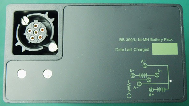
Military Batteries : Ni-Mh Battery Pack BB-390/U
Besides ,the military always have a strict standard on low power self-consuming and deep life cycles .so these above standard has made it special from the other Lithium Battery Pack or other battery packs which applied to life .
Military Batteries
Military Batteries,Military Battery,Military Vehicle Battery,Military Solar Battery
YFJ TECHNOLOGY (HK) CO.,LIMITED , http://www.yfjpower.com