Regarding the FPGA-based DDR3 six-channel read-write protection in the accelerated processing of futures market data...
In the FPGA-based accelerated processing of futures market data, different message types are processed in parallel, and each processing result needs to use memory to cache market data information. The market data information capacity is huge, and the on-chip storage is difficult to meet the demand. Using DDR3 SDRAM has become the preferred method. However, because DDR3 has only one set of data access channels, it cannot meet the demand for simultaneous access of multiple channels. In the previous multi-channel solutions for SDRAM, such as the NPI bus-based off-chip memory designed by Cao Yijiang, the maximum bandwidth can reach 743 Mb/s; Fan Bo and others use the UI interface, and the maximum bandwidth of DDR3 communication can reach 3.8 Gb/ s; Although the transmission rate of the AXI4-based DDR3 multi-port solution designed by Zhang Yujia has increased, the complexity of the AXI4 protocol has increased the difficulty of development and use. This paper implements and verifies the FPGA-based DDR3 six-channel UI interface read and write anti-collision design in the acceleration processing of futures market data, which simplifies the complexity of DDR3 multi-channel read and write. With the improvement of the effective data cycle, the maximum port rate can reach 5.0 Above GB/s, the bandwidth utilization rate can reach over 80%.
1 Overall design architectureThe six-channel read-write anti-collision architecture designed in this paper is shown in Figure 1, which mainly includes a channel arbitration arbitration module, a read-write logic control module, and a DDR3 memory control module.
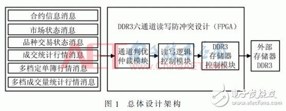
The DDR3 memory controller module uses Xilinx's MIG core. Users only need to select the memory chip through the GUI of the IP core and set the relevant parameters to complete the configuration of DDR3.
The channel arbitration arbitration module will arbitrate the six channels. For different channels with read and write requests at the same time, the module determines the order of access to DDR3 according to the priority level, and uses the interrupt idea to solve the conflict problem of multi-channel read and write.
The read-write logic control module controls the interface generation of DDR3, completes the timing control of the corresponding interface according to different operations, and then realizes the correct read-write access to DDR3.
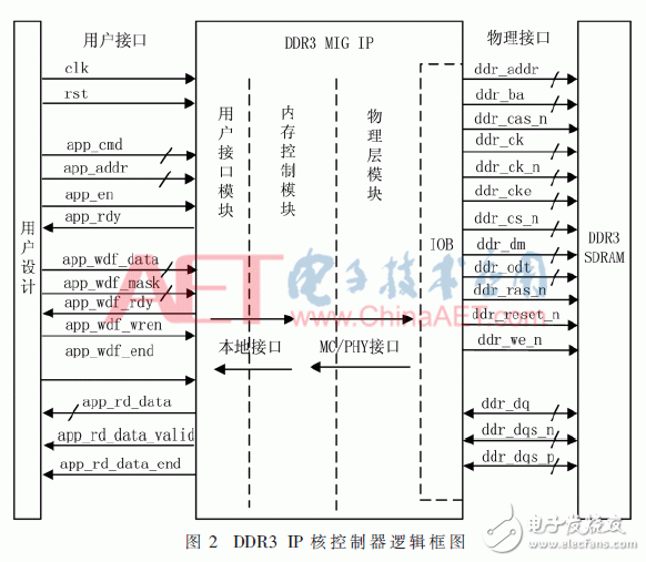
2 DDR3 memory control module designThe logic block diagram of the controller generated by the DDR3 IP core is shown in Figure 2. Compared with the AXI4 interface, the UI interface method does not need to organize the data by yourself and is easy to operate, which greatly simplifies the use complexity of DDR3. It's convenient.
2.1 Storage control module write operation
DDR3 write operation interface signals are shown in Table 1.
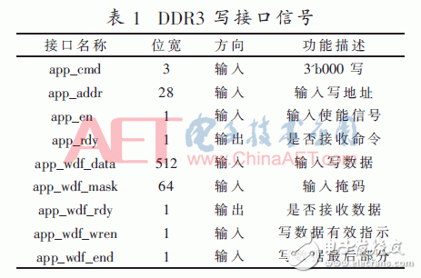
Write operation process: when app_rdy and app_wdf_rdy are both high, the address app_addr written to DDR3 is bound to align with app_cmd, the data written to DDR3 app_wdf_data is bound to the data mask app_wdf_mask, and app_cmd is set to 3′b000, and At the same time, app_en, app_wdf_wren, and app_wdf_end are set high, and the data can be written to the corresponding address.
Because there is more than one write timing for DDR3, in order to simplify system design, the user interface write timing designed in this article is completely aligned with address and data, which is easy to understand and operate.
2.2 Storage control module read operation
The read operation interface signal of DDR3 is shown in Table 2.
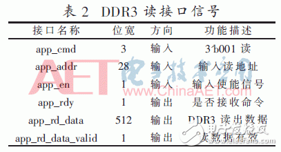
Read operation process: when app_rdy is high, the user sends a read command and sets app_en high at the same time, the read command and read address will be written to DDR3, DDR3 will return data and valid indication signal, both of which determine whether the returned data is effective.
Normally, the data will not be returned immediately after the DDR3 read request ends, and a certain clock cycle needs to be delayed.
3 channel arbitration arbitration module designNormally, because DDR3 has only one set of control, address and data buses, only one channel can be accessed at the same time. According to the processing rules of futures trading, the order of priority from high to low is contract information message, market status message, variety trading status message, transaction statistics market message, multi-file order book market message, and multi-file transaction volume statistics market message. In the process of channel arbitration, first encapsulate the 6 different messages and register them in the corresponding message buffer. Each channel writes the data format in the message buffer. From high to low, it is write enable and read. Enable, write data, write address, read address; then first determine whether the contract information message buffer is empty, if not empty, it proves that there is a request for contract information message, and then the state opportunity jumps to contract information message processing State: After all the buffers of contract information messages are read, it is judged again whether other message buffers are empty in the order of priority, and the state machine then makes corresponding jumps to complete the switching between different channels, as shown in Figure 3.
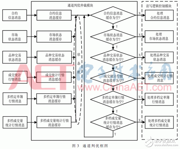
For different message types, corresponding to different message processing units, the purpose is to increase the parallel processing operations of the system and reduce processing delay.
4 Read and write logic control moduleThe read-write logic control module mainly parallelizes different types of messages and generates DDR3 interface signals. The processing flow of each message is shown in Figure 4.
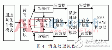
There are many types of contract quotations in futures trading, but they occupy a small space. Usually, one address in DDR3 can complete the storage of one quotation. In the restoration, calculation, and release of the quotation, multiple quotations need to be read. Since the burst length of DDR3 is 8, in order to facilitate accurate access to the market, the data width of the 6 channels is set to 1/8 of the DDR3 bit width, that is, only one address data is accessed at a time.
For the data output by the channel arbitration module, the write enable and read enable are both 1 bit wide, and a high level indicates that a request has occurred; the write data is 64 bits wide; the write address and read address are 28 bits wide. The data bit width of DDR3 is configured as 512 bit in the IP core, and the address bit width is 28 bit. Because the write data bit width does not match the DDR3 data bit width, the DDR3 write operation needs to be completed with the mask.
The processing process is as follows: first, read and write judgments, if the write enable is set high, then jump to the write operation state; if the read enable is set high, then jump to the read operation state, if there is no read or write operation, it is in the waiting state. (In the processing of futures market information, there will be no simultaneous reading and writing of the same channel, so the situation where the read and write enable of the same channel are both high will not occur.)
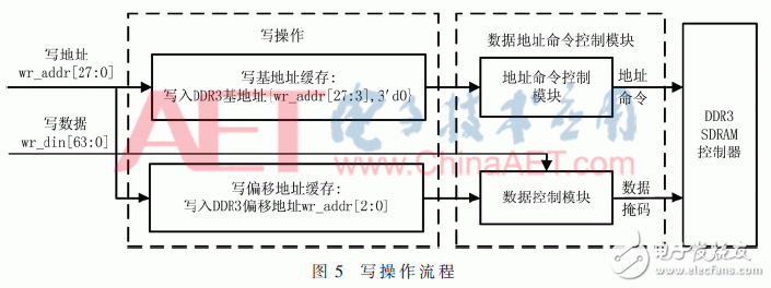
If it is a write operation, on the one hand, generate the address and command to write to DDR3, on the other hand, encapsulate the write data into a 512 bit width. The address app_addr written into DDR3 is {write address [27:3], 3'd0}, and the written data app_wdf_data and mask app_wdf_mask are determined by the write address [2:0]. The data address command control module will also generate app_en, app_wdf_wren, and app_wdf_end control signals correspondingly. These signals work together on the DDR3 SDRAM memory to complete the DDR3 write operation, as shown in Figure 5.
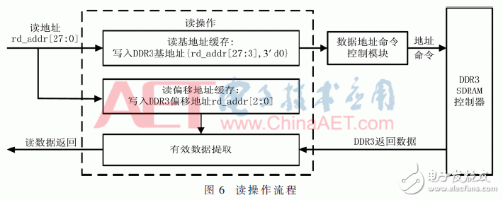
If it is a read operation, the address command selection module assigns the read address [27:3] to app_addr as the base address for writing to DDR3, and at the same time stores the read address [2:0] as the offset address for writing to DDR3 in the corresponding channel In the offset address cache, the data address command control module generates other control signals and transmits them to the DDR3 SDRAM memory. DDR3 SDRAM returns corresponding 512-bit wide data according to the address. While returning the data, read the offset address in the corresponding channel offset address buffer, and extract the corresponding 64 bit data according to the offset to complete a read operation of DDR3, as shown in Figure 6.
5.1 Experimental results
This article uses the Kintex-7 series XC7K325T FPGA chip of Xilinx Company and the JBF9C256x72AKZ DDR3 chip of Micron Company as the hardware platform to verify the correctness of the design in this article and analyze its performance.
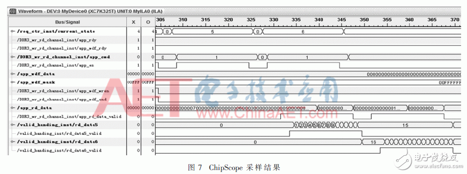
Test method: Six channels initiate DDR3 read and write requests at the same time, of which channels 1 to 4 are for DDR3 write requests, and channels 5 and 6 are for DDR3 read requests. The state machine performs state jumps in order of message priority. Processing, and finally return the data to the corresponding channels respectively, the ChipScope results are shown in Figure 7.
5.2 Experimental analysis
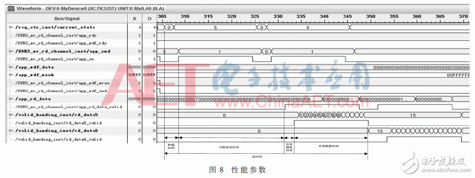
In order to better describe the performance of the design, this article introduces the following parameters. Arbitration time: the time interval from the occurrence of the request signal to the beginning of the channel processing; IP core processing time: the time from the DDR3 IP core receiving the instruction to the return data; the effective extraction time: the time to extract the corresponding 64 bit from the 512-bit DDR3 return data Interval; valid data time: the effective maintenance time of the data; total time: the time from the message request to the data return, that is, the sum of the arbitration time, the IP core processing time and the valid data time. therefore:

In this design, the measured arbitration time is 3 clock cycles, the IP core processing time is 22 clock cycles, and the effective extraction time is 2 clock cycles, as shown in Figure 8.
The effective data time of each channel is different, and the performance is also different. The specific test results are shown in Table 3.

The test results show that the design can complete multi-channel access to DDR3 stably and efficiently. With the improvement of the effective data cycle, the channel rate can reach more than 5 GB/s, and the bandwidth utilization rate can reach more than 80%, which can meet the futures market data. Real-time requirements during processing.
6 ConclusionThis article designs and implements an FPGA-based DDR3 six-channel read-write anti-conflict design, which can effectively solve the conflict problem of multi-channel simultaneous access to DDR3 in the futures market data processing, and the futures market data processing on the existing Kintex-7 series FPGA platform Good application effects have been achieved in the system. The test results show that the anti-collision design can efficiently and correctly complete multi-channel access to DDR3, and has the characteristics of good stability, fixed arbitration time, and high efficiency. The DDR3 multi-channel read and write anti-collision design designed in this paper simplifies the complexity of multi-channel read and write DDR3, reduces the delay in the processing of futures market data, and improves the parallel processing speed.
Installation Accessory,Encoder Sensor With Coupling,Encoder Sensor Wheel,Sensor Encoder
Yuheng Optics Co., Ltd.(Changchun) , https://www.yhenoptics.com