Power supply and grounding design of WiFi transceiver
Power supply and grounding design of WiFi transceiver
Abstract: Reliable RF layout should be based on understanding the basic principles of circuit board structure, power wiring and grounding. This article discusses the relevant basic principles, and provides some practical, proven power wiring, power bypass and grounding techniques, which can effectively improve the performance indicators of RF design. Considering that the PLL spurious signal in the actual design is very sensitive to the power supply coupling, grounding, and the position of the filter element, this article focuses on the method of PLL spurious signal suppression. To illustrate the problem, this article uses the PCB layout of the MAX2827 802.11a / g transceiver as a reference design.
When designing an RF circuit, the design of the power circuit and the layout of the circuit board are often left after the design of the high-frequency signal path is completed. For a design that has not been well thought out, the power supply voltage around the circuit is prone to erroneous output and noise, which negatively affects the system performance of the RF circuit. Reasonable distribution of PCB layers, the use of star topology VCC leads, and the addition of appropriate decoupling capacitors on the VCC pins will help improve the performance of the system and obtain the best indicators.
Reasonable PCB layer allocation is convenient for simplifying the subsequent wiring processing. For a four-layer PCB (a circuit board commonly used in WLAN), in most applications, components and RF leads are placed on the top layer of the circuit board, and the second layer is used as a system ground The power supply part is placed on the third layer, and any signal line can be distributed on the fourth layer. The use of an undisturbed ground plane layout for the second layer is necessary to establish an impedance-controlled RF signal path. It is also convenient to obtain the shortest possible ground loop, providing a high degree of electrical isolation for the first and third layers, making the two The coupling between layers is minimal. Of course, other board layer definition methods can also be used (especially when the circuit board has different layers), but the above structure is a successful example that has been verified.
A large-area power layer can make VCC wiring easier, but this structure is often a fuse that deteriorates the performance of the system. Connecting all power leads together on a large plane will inevitably avoid the pin between the pins. Noise transmission. Conversely, if a star topology is used, the coupling between different power supply pins will be reduced. Figure 1 shows the star-connected VCC wiring scheme, which is taken from the evaluation board of the MAX2826 IEEE 802.11a / g transceiver. In the figure, a main VCC node is established. From this point, the power lines of different branches are led to supply power for the power pins of the RF IC. Each power supply pin uses an independent lead to provide spatial isolation between the pins, which is helpful to reduce the coupling between them. In addition, each lead also has a certain parasitic inductance, which is exactly what we want, it helps filter out high-frequency noise on the power line. 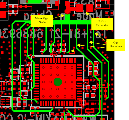
Figure 1. Star topology VCC wiring
When using star topology VCC leads, it is necessary to take appropriate power supply decoupling, and there is a certain parasitic inductance in the decoupling capacitor. In fact, the capacitor is equivalent to a series RLC circuit. As shown in Figure 2, the capacitor plays a dominant role in the low frequency band, but at the self-oscillation frequency (SRF)  After that, the impedance of the capacitor will appear inductive. It can be seen that the capacitor has a decoupling effect only when the frequency is close to or lower than its SRF, and the capacitance shows low resistance at these frequency points. Figure 3 shows the typical S11 parameters under different capacitance values. From these curves, it can be clearly seen that their SRF, and the larger the capacitance, the better the decoupling performance provided at lower frequencies (presented The lower the impedance).
Figure 2. The equivalent circuit of a capacitor 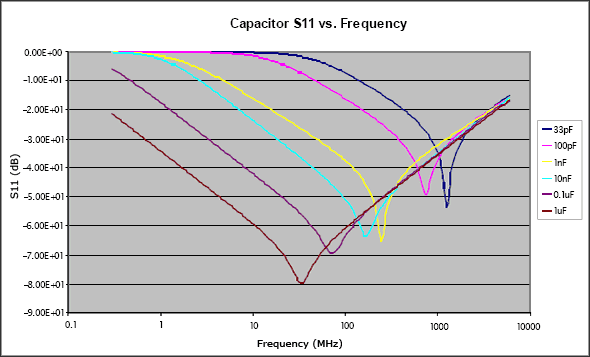
Figure 3. Capacitor impedance changes at different frequencies
It is best to place a large-capacity capacitor at the main node of the VCC star topology, such as 2.2µF. This capacitor has a low SRF and is effective for eliminating low-frequency noise and establishing a stable DC voltage. Each power pin of the IC requires a low-capacity capacitor (such as 10nF) to filter out high-frequency noise that may be coupled to the power line. For power supply pins that supply power to noise-sensitive circuits (for example, VCO power supplies), two bypass capacitors may be required. For example, using a 10pF capacitor in parallel with a 10nF capacitor to provide bypass can provide a wider frequency range of decoupling, try to eliminate the impact of noise on the power supply voltage. Each power supply pin needs to be carefully tested to determine how much decoupling capacitors are needed, and at what frequency the actual circuit is susceptible to noise interference.
Good power supply decoupling technology combined with rigorous PCB layout and VCC leads (star topology) can lay a solid foundation for any RF system design. Although there will be other factors in the actual design that reduce the system performance indicators, having a "noise-free" power supply is the basic element for optimizing system performance.
The layout and leads of the ground plane are also the key to the design of the WLAN circuit board. They directly affect the parasitic parameters of the circuit board, and there is a hidden danger of reducing the system performance. There is no unique grounding scheme in RF circuit design. There are several ways to achieve satisfactory performance indicators in the design. The ground plane or lead can be divided into analog signal ground and digital signal ground, and can also isolate circuits with large current or large power consumption. According to the previous design experience of the WLAN evaluation board, using a separate ground plane in the four-layer board can get better results. With these experiences, using the ground layer to isolate the RF part from other circuits can avoid cross-interference between signals. As mentioned above, the second layer of the circuit board is usually used as a ground plane, and the first layer is used to place components and RF leads.
After the ground layer is determined, connect all signal grounds to the ground layer with the shortest path. Usually, the vias are used to connect the top layer ground wire to the ground layer. It should be noted that the vias appear inductive. The physical model of the via is shown in Figure 4. Figure 5 shows the precise electrical characteristics model of the via, where Lvia is the via inductance and Cvia is the parasitic capacitance of the via PCB pad. If the ground layout technique discussed here is used, the parasitic capacitance can be ignored. A 1.6mm deep via with an aperture of 0.2mm has an inductance of about 0.75nH, and the equivalent reactance in the 2.5GHz / 5.0GHz WLAN band is about 12Ω / 24Ω. Therefore, a ground via does not provide true grounding for RF signals. For high-quality circuit board designs, as many ground vias as possible should be provided in the RF circuit section, especially for bare ground in general IC packages Pad. Poor grounding will also generate radiation at the receiving front end or power amplifier section, reducing the gain and noise figure specifications. It should also be noted that poor soldering of the ground pad can cause the same problem. In addition, the power consumption of the power amplifier also requires multiple vias connected to the ground layer. 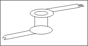
Figure 4. Physical model of the via 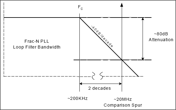
Figure 5. Electrical model of vias
Filter out the noise of other circuits and suppress the locally generated noise, thereby eliminating the cross-interference between the stages through the power line. This is the benefit of VCC decoupling. If the decoupling capacitor uses the same ground via, due to the inductive effect between the via and ground, the vias at these connection points will carry all the RF interference from the two power supplies, not only losing the function of the decoupling capacitor, but also It also provides another path for inter-stage noise coupling in the system.
In the discussion in the third part of this article, we will see that the implementation of PLL always faces huge challenges in system design. To obtain satisfactory spurious characteristics, you must have a good ground layout. At present, all PLLs and VCOs are integrated into the chip in IC design. Most PLLs use digital current charge pump output to control the VCO through a loop filter. Usually, it is necessary to filter the digital pulse current of the charge pump with a second- or third-order RC loop filter to obtain an analog control voltage. The two capacitors close to the output of the charge pump must be directly connected to the ground of the charge pump circuit. In this way, the pulse current path of the ground loop can be isolated to minimize the corresponding spurious frequency in the LO. The third capacitor (for the third-order filter) should be directly connected to the ground plane of the VCO to avoid the control voltage floating with the digital current. If these principles are violated, a considerable amount of stray components will result.
Figure 6 shows an example of PCB layout. There are many ground vias on the ground pad, allowing each VCC decoupling capacitor to have its own ground via. The circuit in the box is a PLL loop filter. The first capacitor is directly connected to GND_CP, the second capacitor (in series with an R) is rotated 180 degrees and returns to the same GND_CP, and the third capacitor is connected to GND_VCO. This grounding scheme can achieve higher system performance. 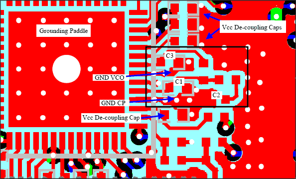
Figure 6. Example of PLL filter component placement and grounding on the MAX2827 reference design board
Meeting the requirements of the 802.11a / b / g system to transmit the spectrum mask is a difficult point in the design process. It is necessary to balance the linear index and power consumption, and leave a certain margin to ensure that it meets the IEEE while maintaining sufficient transmit power And FCC regulations. The typical output power required by the IEEE 802.11g system at the antenna end is + 15dBm, and -28dBr when the frequency deviation is 20MHz. The power rejection ratio (ACPR) of adjacent channels in the frequency band is a function of the linear characteristics of the device, which is correct for a specific application under certain premises. Much work in optimizing ACPR characteristics in the transmission channel is achieved by adjusting the bias of the Tx IC and PA, and tuning the matching network of the input stage, output stage, and intermediate stage of the PA.
However, not all the problems that cause ACPR are attributed to the linearity of the device. A good example is: after a series of adjustments, optimization of the power amplifier and PA driver (the two factors that play a major role in ACPR) The adjacent channel characteristic of the WLAN transmitter still cannot reach the expected index. At this time, it should be noted that the spurious signal from the transmitter phase-locked loop local oscillator (LO) will also deteriorate the ACPR performance. The spurious signal of LO will be mixed with the modulated baseband signal, and the mixed components will be amplified along the expected signal path. This mixing effect will only cause problems when the PLL spurious content is above a certain threshold. When it is below a certain threshold, ACPR will be mainly restricted by the nonlinearity of the PA. When the Tx output power and spectrum mask characteristics are "linearly limited", we need to balance the linearity index and the output power; if the LO spurious characteristics become the main factor restricting ACPR performance, we will face "spurs" "Limited", it is necessary to bias the PA at a higher operating point under the specified POUT to reduce its impact on ACPR, which will consume more current and limit the flexibility of the design. 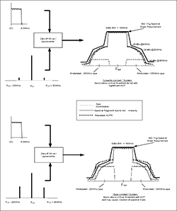
Click to enlarge. Figure 7. Performance degradation due to 802.11a / b / g spectrum mask and spurs
The above discussion raises another question, that is, how to effectively limit the PLL spurious content to a certain range so that it does not affect the emission spectrum. Once the spurious component is found, the first thought is to narrow the bandwidth of the PLL loop filter in order to attenuate the amplitude of the spurious signal. This method is effective in rare cases, but it has some potential problems.
Figure 8 shows a hypothetical situation, assuming a N-frequency synthesizer with a relative frequency of 20MHz is used in the design. If the loop filter is second-order, the cutoff frequency is 200kHz, and the roll-off rate is usually 40dB / ten. In octave, 80dB attenuation can be obtained at 20MHz. If the reference spurious component is -40dBc (assuming the level that can cause harmful modulation components), the mechanism of generating spurious may exceed the range of the loop filter (if it is generated before the filter, its amplitude may be very Big). The bandwidth of the compression loop filter will not improve the spurious characteristics, but will increase the PLL phase lock time, which will have a significant negative impact on the system. 
Figure 8. Simplified PLL filter asymptote, corresponding corner frequency and spurious location
Experience has shown that the effective way to suppress PLL spurs is reasonable grounding, power layout, and decoupling techniques. The routing principles discussed in this article are a good starting point for reducing PLL spurious components. Considering the large current changes in the charge pump, it is necessary to adopt a star topology. If there is not enough isolation, the noise generated by the current pulse will couple to the VCO power supply and modulate the VCO frequency, which is usually called "VCO traction". Measures such as physical separation between power lines and decoupling capacitance of each VCC pin, proper placement of ground vias, and introduction of a series ferrite element (as a last resort) can improve isolation. The above measures do not need to be used in every design. Appropriate use of each method will effectively reduce the spur amplitude.
Figure 9 provides a result of the unreasonable VCO power supply decoupling scheme. The power supply ripple indicates that it is the switching effect of the charge pump that causes strong interference on the power supply line. Thankfully, this strong interference can be effectively suppressed by adding bypass capacitors. Figure 10 shows the measurement results at the same point after the circuit is changed. 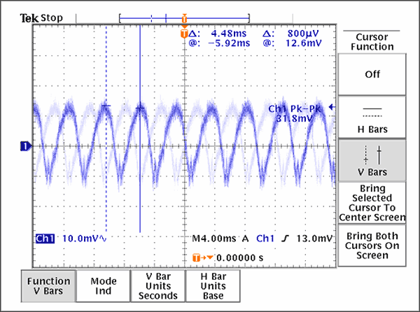
Figure 9. Unreasonable VCC_VCO decoupling test results 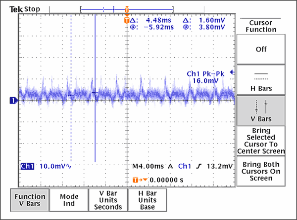
Figure 10. Adding bypass capacitors at the VCO power supply reduces noise.
In addition, if the power supply wiring is unreasonable, for example, the power lead of the VCO is located just below the charge pump power supply, the same noise can be observed on the VCO power supply. The generated spurious signal is sufficient to affect the ACPR characteristics. The results will not be improved. In this case, it is necessary to examine the PCB layout and rearrange the power leads of the VCO, which will effectively improve the spurious characteristics and meet the specifications required by the specification.
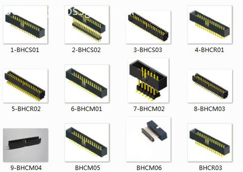
Antenk box header connector,Those products are used in more or less every known application within computer-, industrial-, telecommunication and specific automotive markets. This product technology allows cost effective connections between printed circuit boards based on removable or permanent connections based on a longterm proofed way of assembly. box header connectors are available with the traditionally used pitch of 2.54mm and the pitch of 2.00mm,1.27mm.
Antenk Box header/Ejector header Description and Application:
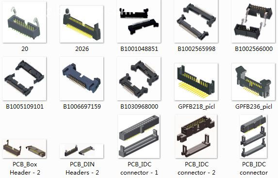
Box header/ ejector header connector, With DIP straight/vertical, SMT,Right angle, 2.54pitch, 2.0pitch, 1.27pitch,
The commonly used Pin ways have 6P,8P,10P,14P,16P,20P, 24P,26P,30P,34P, 40P,50P,64P.
Box header/ ejector header and IDC Flat Cable connectors are two of the most commonly used connectors. Box headers can be found in nearly all electronic equipments.
This is a IDC product which allows cost effective connections between circuit boards based on permanent connection (using transition connector) or removable connection
(Using for IDC flat cable connectors).
Box header
Ejector header
Box Header,Box Header Connectors,Ecu Box Header Connector,Latch Box Header Connector,1.27mm Box Header Connector,2.00mm Box Header Connector,2.54mm Box Header Connector
ShenZhen Antenk Electronics Co,Ltd , https://www.antenkconn.com