Monolithic integrated variable gain visible light receiver solution (1)
1 circuit design
1.1 The overall design of the circuit
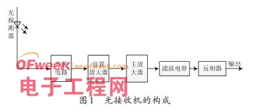
As shown in Figure 1, the optical receiver of this design consists of a photodetector, a switching circuit, a preamplifier, a main amplifier, a filter capacitor, and an inverter. Due to the influence of natural light, the detector also has a weak current output when transmitting data 0. Therefore, the amplifier must be strictly controlled in a reasonable range during design, which must satisfy the high level amplification and avoid the low level. The amplification voltage is reached after amplification.

1.2 Photodetector
The photodetector of this design is a dual photodiode DPD structure that uses N wells to shield substrate carriers. Ion implantation used to achieve source and drain regions in the CMOS process is used to form the anode and cathode of the DPD. The manufacturing method is to make a P+ interdigitated electrode in the N well, and use the N+ diffusion to extract the N well electrode, and the N well is surrounded by the P+ protection ring. The P+ interdigitated structure is arranged to increase the width of the depletion region and make the electric field of the depletion region more uniform, so as to facilitate more rapid drift of the photogenerated carriers.
According to the actual measurement, under normal indoor illumination, the detector output current is between 1.5~3.5 μA due to the different distance from the detector to the light source, and about 0.1 μA output when the light source is turned off.
1.3 Switch circuit
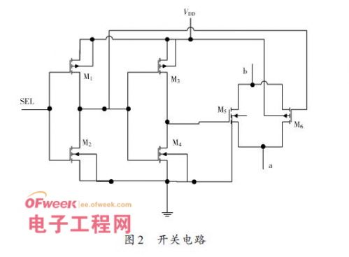
Since this monolithic integrated design is used, a switching circuit is added between the detector and the amplifying circuit in order to prevent the detector from inputting current to the amplifying circuit for a long time. The switching circuit design is shown in Figure 2. The a and b terminals are connected to the detector and the amplifier respectively. When the SEL is connected to a high potential, the switching circuit is turned on, and vice versa.

Since the switching circuit is equivalent to a short circuit when it is turned on, no additional capacitance or resistance is introduced, and the bandwidth is much higher than that of the main body of the amplifying circuit, so that it does not affect the circuit.
1.4 Preamplifier
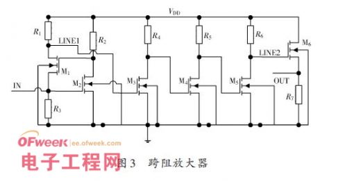
To convert the current signal into a voltage signal, an effective solution is to use a transimpedance type preamplifier. The transimpedance amplifier has the advantages of gain stability, frequency bandwidth, and no equalization circuit. The design structure is shown in Figure 3.

In order to isolate large parasitic capacitance and increase bandwidth, this design uses the RGC structure shown in Figure 4 as the input stage. The input resistance of the RGC is: 

Power 30W ,output voltage 3-12V, output current Max 1.2A , USB output 5v 2a, 6 dc tips. We can meet your specific requirement of the products, like label design. The material of this product is PC+ABS. All condition of our product is 100% brand new.
Our products built with input/output overvoltage protection, input/output overcurrent protection, over temperature protection, over power protection and short circuit protection. You can send more details of this product, so that we can offer best service to you!
30W Wall Adapter ,30W Wall Power Supply,30W Power Cord In Wall, 30W Wall Power Adapter
Shenzhen Waweis Technology Co., Ltd. , https://www.waweisasdapter.com