Design of high-speed data transmission system based on FPDP
Design of high-speed data transmission system based on FPDP
With the rapid development of electronic technology, more and more signal processing systems require high-speed data acquisition and large-throughput data transmission to achieve high-speed real-time data processing capabilities. In the radar system, the raw data contains rich information. It is particularly important to obtain the raw data and analyze it in real time. Therefore, it is necessary to use a large number of inter-board communication in the radar processor, and to ensure that the data transmission between the boards is high-speed and reliable Sex. The single-board system can no longer meet the demand and needs to be implemented by multiple boards.
The FPDP bus can be used for high-speed data transmission between two or more VME boards, and its data transmission rate can reach 160 MB / s. The FPDP bus is located on the front panel of the VME board, and does not affect the VME bus located in the backplane slot at all. In practical applications, a VME board allows multiple FPDP ports. Therefore, in the radar system, the use of the FPDP bus will certainly improve data transmission and processing capabilities.
1 FPDP bus overview
The FPDP (Front Panel Data Port, front panel data port) bus was originally developed by InteracTIve Circuits and Sys-tems Ltd (ICS) of Canada, and then proposed and formed a standard agreement by VSO (VITA Stand-ards OrganizaTIon). The FPDP bus is a 32-bit parallel synchronous bus, which is connected between boards through an 80-core flat connection cable. Mainly used for high-speed data transmission between two or more VME bus boards.
The devices on the FPDP bus can have:
(1) FPDP master sending device (FPDP / TM: FPDP Transmitter Master), the master sending device is the source end of data transmission, and generates clocks and related timing signals required by all other boards;
(2) FPDP master receiving device (FPDP / RM: FPDP Re-ceiver Master), the master receiving device is the end of data transmission, used to receive data and terminate control signals;
(3) FPDP receiving device (FPDP / R: FPDP Receiv-er), the receiving device only receives data, without terminating the control signal, allowing the data transmission to continue.
There must be at least one master sending device and one master receiving device on the FPDP bus. However, there can be multiple receiving devices, so that "multipoint" transmission can be achieved. At a certain moment, there is only one master sending device in the bus, and the transmission is performed in one direction, so there is no bus competition and conflict between the devices on the bus. Therefore, the FPDP bus protocol does not include the address and arbitration cycle, so that high-speed data transmission can be achieved.
Although the FPDP bus is a unidirectional transmission, the sending device and the receiving device of the FPDP bus can be configured through hardware link switches or software means to realize time-multiplexed bidirectional data transmission.
2 Design examples
In a radar system, the changes in the original data (state parameters such as distance, square, speed, etc. of the target) have a very important influence on the imaging results. Therefore, the ability to transmit the collected raw data in real time and perform effective analysis will directly affect the quality of imaging.

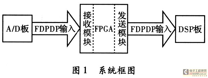
In this design, the data channel of FPGA adopts FPDP bus structure, which is connected with A / D board and DSP board, respectively, for real-time high-speed data transmission. The A / D board is responsible for high-speed acquisition of the echo signal, and the DSP board receives the synthesized data sent by the FPGA for post-processing. The FPDP receiving module is responsible for receiving the original echo data from the A / D board, and the FPDP sending module is responsible for packaging the original echo data and other aircraft parameters and sending them to the DSP board in the form of the FPDP protocol. As shown in Figure 1.
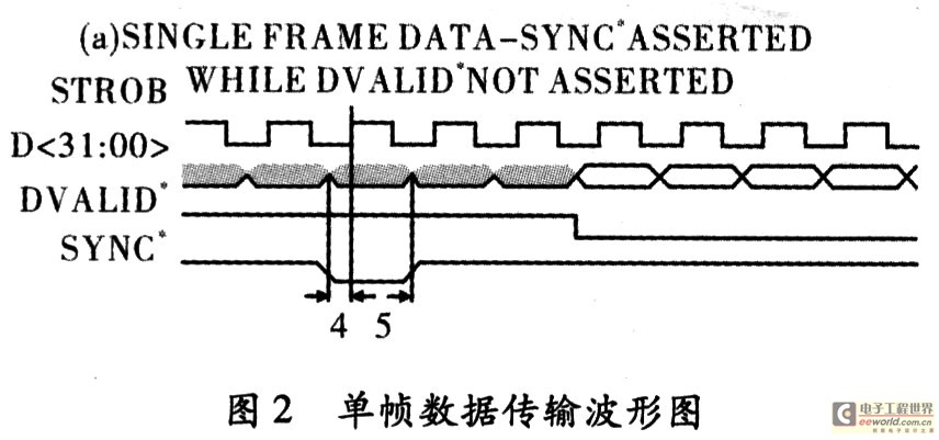
The data interfaces of the A / D board and the DSP board are all FPDP bus structures, and the transmission mode is a single frame mode. For the single-frame data transmission mode, the synchronization signal SYNCn should precede the first data sent. At this time, the data valid signal (DVALIDn) is still high, indicating that the data is invalid. During data transmission, the DVALIDn signal is valid, and the transmission data is driven to the data bus of the FPDP under the synchronization of the rising edge of the clock STROB (or PSTROBE). At the rising edge of the clock STROB (or PSTROBE), the receiving device pairs D [31. . 0] and DVALIDn signal for sampling. If DVALIDn is low, the sent data is considered valid. Single frame data transmission waveform diagram, as shown in Figure 2.

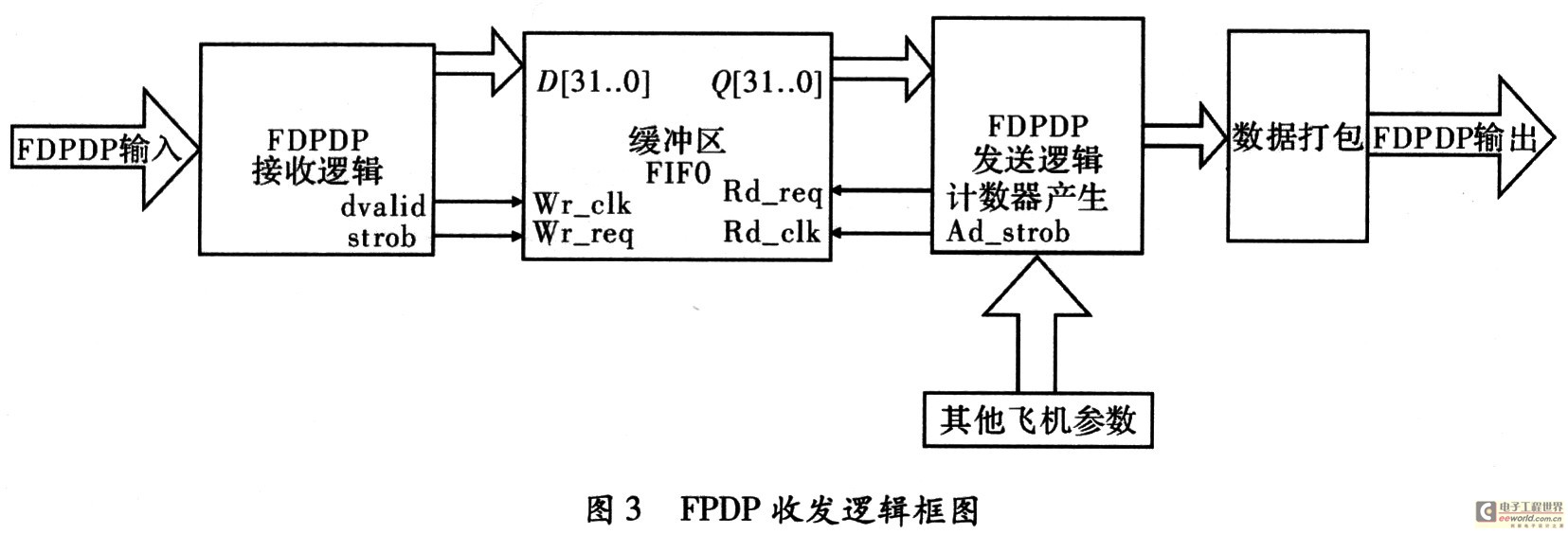
In order to meet the real-time processing requirements of the signal processor, the original data input to the DSP board is required to conform to the processed data format. The collected data needs to be packaged in a certain format, which is called data synthesis. FPGA should synthesize the data from different devices into the required frame format and then forward it to the DSP board. In this way, after the DSP board obtains the data frame, it can be directly processed without the overhead of format conversion. The schematic diagram is shown in Figure 3.

Due to the strong real-time requirements of FPDP bus transmission, data loss is not allowed in the transmission process, which has the characteristics of large data volume and high transmission speed. Therefore, the FPDP receiving logic should send it to the DSP board as soon as possible after receiving the original echo data. Otherwise, it will cause data jam, loss and disorder, which will seriously affect the back-end imaging processing, so a data buffer FIFO is introduced between the FPDP bus transceiver logic to temporarily store the original echo data.
The FPDP receiving logic receives the echo data from the A / D board and is mainly responsible for the write operation to the data buffer FIFO. The working process is as follows: When the FPDP bus data is valid (DVALIDn is low), the FIFO write request Wr-req signal is valid, and the data follows the write clock signal (Wr-clk is the Ad-strob signal sent from the AD board) Write to FIFO. If the FPDP bus data is invalid, the write request signal of the FIFO is also invalid at this time, and the data cannot be written into the FIFO.
The FPDP sending logic interface is responsible for packaging the echo data and other aircraft parameters according to a certain format and sending them out through the FPDP bus. The work flow is as follows: The read request Rd-req signal of FIFO is generated by the sending timing counter. When the count value of the counter is a certain value (A / D collects a full frame of data), Rd-req is valid. With the read clock (Rd -clk is the A / D board clock AD_strob) signal, the data is read from the FIFO, and the counter is cleared at this time. After the data is packed in a certain format, the packed data is sent to the DSP board according to the FPDP single-frame transmission mode.
The FPDP transmission logic should start data transmission immediately after the FPDP synchronization signal SYNCn arrives, which greatly enhances the real-time and reliability of data transmission. It is worth noting that the first set of echo data from the A / D board is too late to be packaged and sent to the DSP board. Therefore, it is necessary to accumulate a set of echo data in the FIFO before sending data to the DSP board. In a frame of data on the DSP board, the echo data should be the data sent from the last A / D board, so as to ensure that the echo data is not lost, but the last group of echo data will still exist in the timing board, and the acquisition will not It should be discarded.
In particular, because the input and output functions of the module have been determined, the direction signal DIRn as the receiving end of the A / D board is not used, and the DIRn signal as the sending end of the DSP board is often connected low. For the input SUSPENDn and NRDYn signals, the A / D acquisition board does not respond to the NRDYn signal, so the FPGA does not respond to these two signals to avoid interfering with the data acquisition of the AD acquisition board.
3 Design simulation
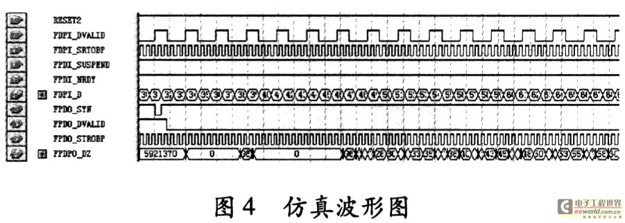
The following gives a waveform simulation diagram based on Quartus 6.0, as shown in Figure 4.

As shown in Figure 4, it is a simulation diagram of FPDP sending logic, in which FPDI_SUSPEND and FPDI_NRDY are always invalid (high), FPDO_SYN is valid (low) before sending data, and FPDO_DVALID is still invalid (high). When transmitting data, FPDO_DVALID is valid (low), and the data is sent out through the FPDP bus at the rising edge of the clock FPDO_STROBP.
4 Conclusion
The following conclusions are drawn from the above analysis:
(1) In this design, the FPDP bus, with its unique front panel mode and transmission mechanism, effectively solves the problem of high-speed data transmission between multiple boards;
(2) The high-speed, real-time reception and transmission of FPDP data is difficult. The design uses an on-chip FIFO buffer to solve this problem. The on-chip FIFO is highly integrated and takes up fewer resources, effectively solving system requirements;
(3) The design uses the synchronization signal as the effective sign of the received frame, which improves the real-time and reliability of the system.
Din Connector,Waterproof Cable Connector,Ip66 Wire Waterproof Connector,Waterproof Power Connector
Shenzhen Hongyian Electronics Co., Ltd. , https://www.hongyiancon.com