A new generation of high-brightness LEDs can be fabricated with proximity exposure devices
Recently, SUSS MicroTec AG disclosed that the approximately 3 μm pattern required for the manufacture of a new generation of high-brightness LEDs can be resolved using existing proximity exposure devices. This is achieved by improving the optical system and illumination of the proximity exposure device, and changing the photomask. With this technology, LED manufacturers are expected to use proximity exposure devices in the development and mass production of next-generation high-brightness LEDs without the need to introduce expensive projection exposure devices such as steppers.
The company is a large-scale manufacturer of proximity exposure devices for MEMS, semiconductor packaging and LEDs. Although the relevant content has not been announced, Tech-On!'s interview shows that among the large LED manufacturers, it is estimated that each company uses dozens to 100 Sussex exposure devices.
A new generation of high-brightness LED manufacturing requires a pattern of about 3 μm in order to prepare a structure that can improve the light extraction efficiency of LEDs on a substrate such as sapphire. This structure needs to be periodically formed in a size of 3 to 4 μm.
The proximity exposure apparatus used in the conventional LED structure cannot form a pattern of about 3 μm. Therefore, it is generally believed in the industry that a projection exposure device such as a stepper is required for mass production of a new generation of high-brightness LEDs.
In an exposure technique capable of achieving a resolution of about 3 μm, in addition to projection exposure, vacuum contact exposure is also available. This is a technique in which a vacuum state is formed between the photo-curing mold and the bottom plate, so that the distance between the two is narrower than the proximity exposure, thereby improving the resolution. However, vacuum contact exposure has a problem of low yield, and it is recognized that it is difficult to use for mass production.
An example of a 2.5 μm square pattern formed. The exposure gap between the photomask and the substrate was 100 μm. There is less passivation in the angular portion. Provided by Suss Micro.
An example of a hexagonal pattern of 5 μm or less formed. The exposure gap was 40 μm. Provided by Suss Micro.
SMO for proximity exposure
Suss Micro disclosed that through the three improvements, a 2.5μm pattern can be formed by using a proximity exposure device: (1) optimization of an optical system such as a new microlens; (2) additional filter optimization lighting system; 3) OPC (Optical Proximity Correction) technology is applied to the photomask. (1) and (2) can be achieved by modifying existing exposure devices. By combining these three improvements, the same SMO (Source Mask Optimization) as the optimization method of the entire exposure process of the cutting-edge semiconductor device is realized.
The optical system improvement in (1) is intended to make the illumination characteristics of the light source more stable. The new microlens array, which can reduce the illumination deviation, can improve the intensity and angular uniformity of the illumination light, and can also eliminate the poor optical factors that cause the light source to be misaligned and the brightness of the light-emitting surface to be uneven.
The lighting system improvement in (2) aims to control the illumination light with high precision. By inserting a filter for illumination, high precision of illumination light is achieved.
(3) OPC is added to prevent image failure and process failure that may occur when pattern exposure of about 3 μm is performed by only the above (1) and (2). As with the OPC for memory and logic LSI, an auxiliary pattern below the image boundary is additionally added to the photomask pattern.
According to the company, when the proximity exposure of about 3 μm is performed by only (1) and (2), the shadow of the Cr pattern formed on the photo-baking mold is easily transferred to the photoresist, and the corner portion of the pattern is passivated. , line width chaos, line end defects, and areas with different pattern densities produce shape confusion due to proximity effects, and so on. (Editor: maysoong)

Low Cost PCB
PCB Fab - High Quality at a Lower Cost
Let BentePCB' buying power work for you in getting you the lowest cost PCBs!
we can provide our customers with the best PCB prices in the industry. Whether you are looking for someone connection to handle your high volumes at the best possible prices; or you have some high technology boards requirements that you want the best deal on we can make it happen; low cost PCBs with high quality customer service.
When it comes to finding the very best prices on the market, let BentePCB find the low cost PCB fabricator that's right for you. A cheap PCB fabrication is not our goal; inexpensive high quality ones are!
Call us at +86-755-8339 3378 or email your request to service@bentepcb.com.
Tell our experts what you need and we will provide you with the right PCB fabrication and assembly solution. We are ready and eager to turn your concepts into reality.
About Us:
BentePCB is a professional PCB manufacturing which is focus on double side, multilayer, HDI PCB, rigid PCB and Flexible PCB mass production. The company was established on 2011.
We have two factories together, The factory in Shenzhen is specialized in small and middle volume orders and the factory in Jiangxi is for big volumn.
Why Us?
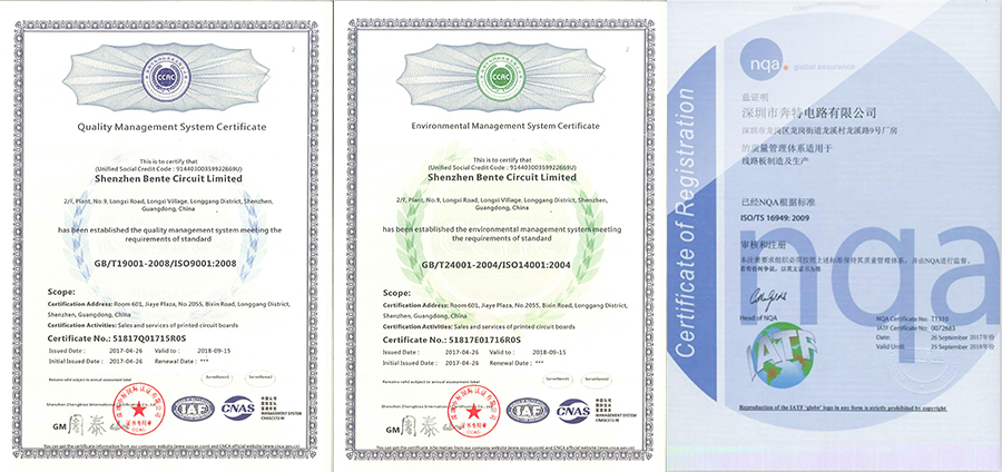
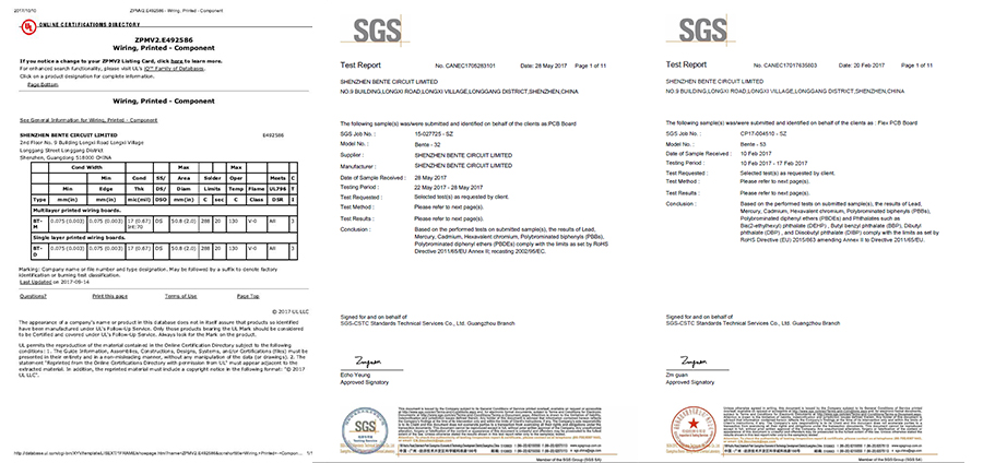
UL (E492586), ISO9001, ISO14001, TS16949, RoHS certified.
Turnover USD 10-50 million per year.
15,000 sqm area, 450 staff .
Mass Production from single to 16 layers.
Special Material:ROGERS, Arlon, Taconic.etc.
Client:Huawei, SAMSUNG, Malata, Midea,Texas Instruments.etc.
Certification(UL:E492586, TS16949, ISO14001, ISO9001,RoHS):
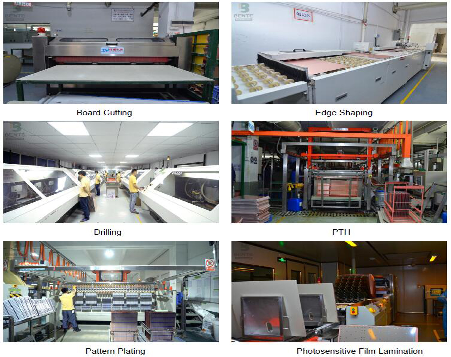
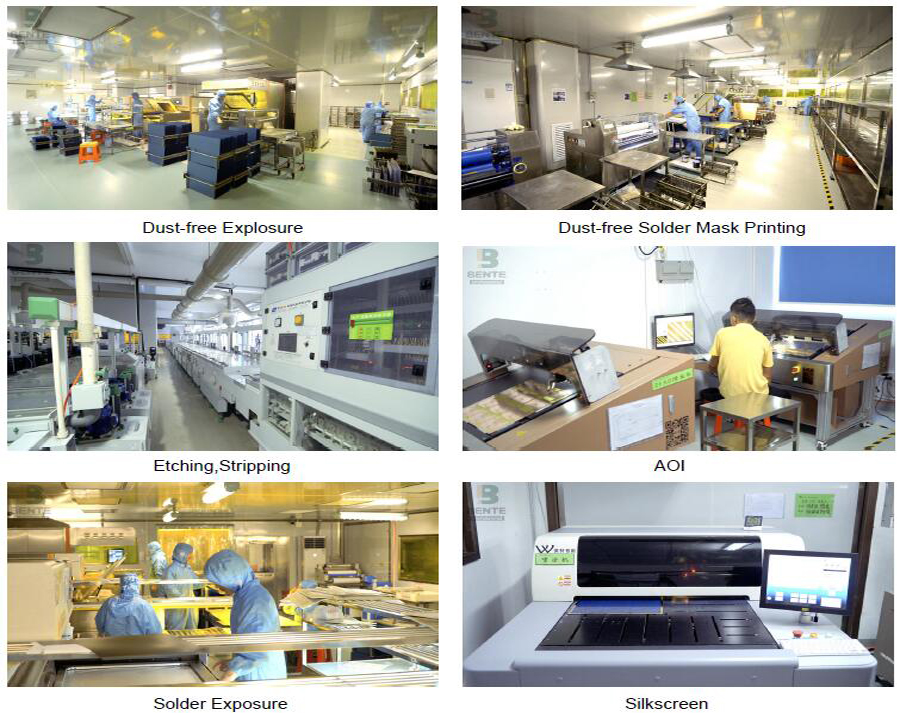
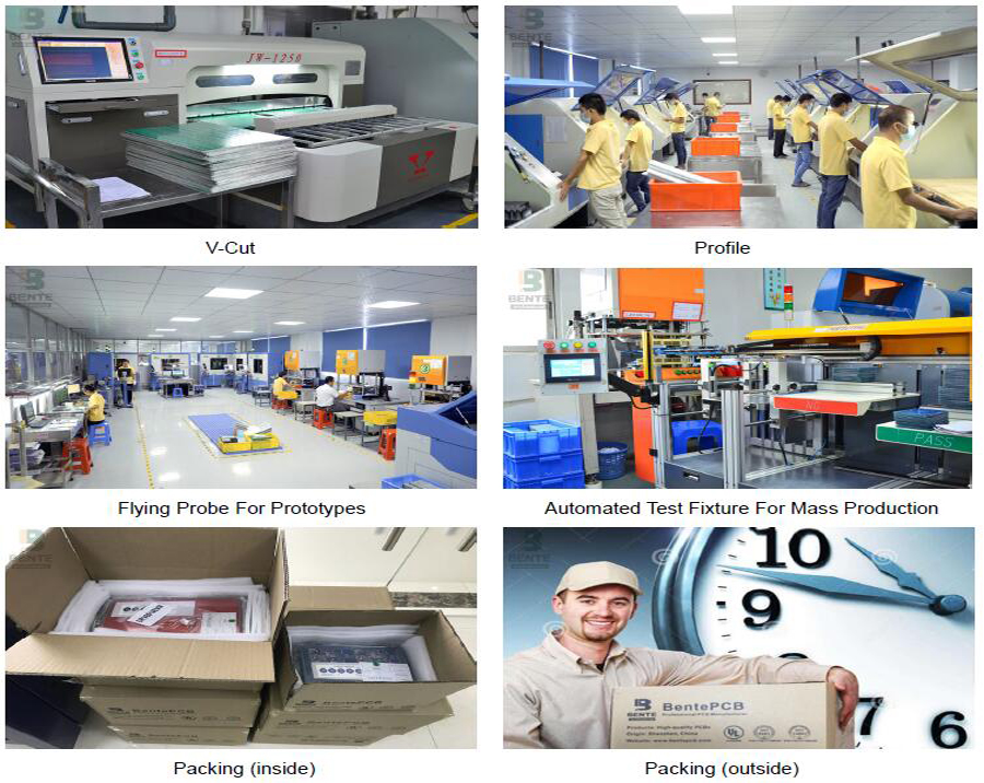
Factory Tour:
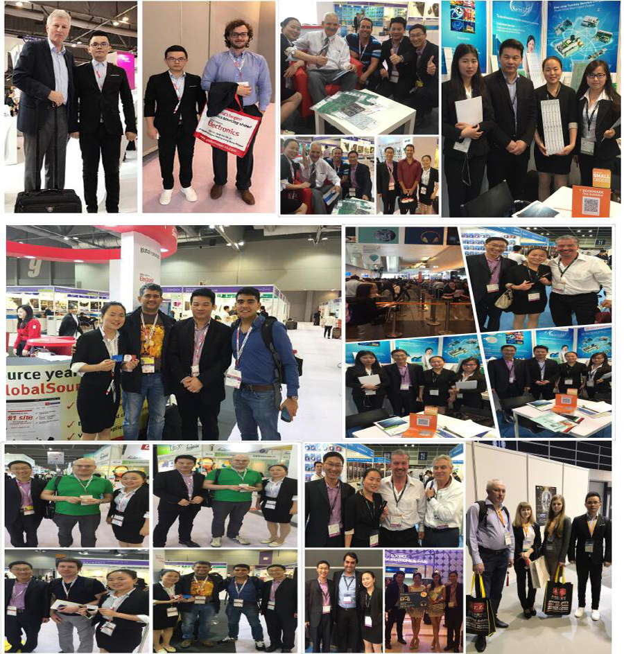
Exhibition:
We Took part in the famous exhibitions over the past years,and got highly appreciation from the top experts,as well as cooperated tightly with them.
Delivery:
BentePCB offers flexible shipping methods for our customers, you may choose from one of the methods below.

FAQ:
Q1: What does BentePCB need for a customized PCB order?
A: The customers need to provide Gerber or pcb file.If you do not have the file in the correct format, you can send all the details related to the products.
Q2: What is your quotation policy?
A: For the PCB order in large quantity, BentePCB will send you the quotation based on the MOQ of the products concerned, and the price will be reasonable with good quality.
Q3: How long will you send us quotation ?
A: After all files were sent, 2 to 8 hours as per your file.
Q4:What is your minimum order quantity?
A:Our MOQ is 1 PCS.
Q5: How about the service BentePCB offered to the customers?
A: If you have any questions about our products or company, do not hesitate to send us your inquiry toour customer service representatives, Your satisfaction is our pursuits.

We don`t just sell PCBs .We sell sleep.

Low Cost PCB
Low Cost PCB, Low Cost PCB Prototype, Low Cost PCB Service, Low Cost PCB Circuit Board
Shenzhen Bente Circuit Limited , http://www.bentegroup.com