4 kinds of packaging materials and 3 package structures to solve the problem of high-power LED heat dissipation
High-power LED package thermal analysis
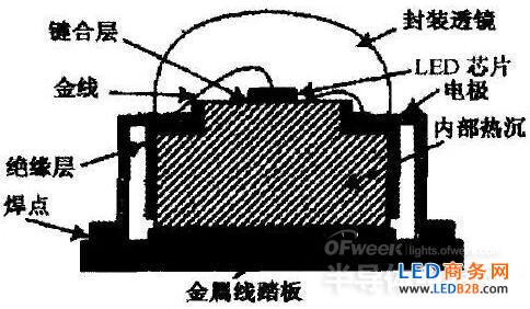
The figure below shows a configuration diagram of the LED package, the package shown in FIG analyzed by dissipation path follows: (1) led Chip - Encapsulated lens - the external environment (2) led chip - bonding layer - internal heat sink - the heat radiation substrate - the external environment ( 3) LED chip - gold wire - electrode - external environment. Since the thermal conductivity of each material inside the package is different, most of the heat is transferred to the external environment through the second heat dissipation path.

The total thermal resistance of the LED package device is represented by the thermal resistance of each link in series:
Rtotal=Rchip+Rchip-TIM+RTIM+RTIM-Cu+RCu+RCu-MCPCB+RMCPCB+RMCPCB-air
Among them, Rchip is the chip thermal resistance, Rchip-TIM is the interface thermal resistance between the chip and the bonding layer, RTIM is the thermal resistance of the bonding layer, and RTIM-Cu is the interface thermal resistance between the thermal interface material and the internal heat sink. RCU is the thermal resistance of the internal heat sink, the RCu-MCPCB is the internal heat sink and the metal wire pedal, the RMCPCB is the thermal resistance of the metal wire pedal, and the RMCPCB-air is the thermal resistance of the metal wire pedal to the air.
It can be seen from the above analysis that the total thermal resistance of the LED package device is formed by a series of multiple thermal resistances. A large number of studies have shown that Rchip-TIM+RTIM+RTIM-Cu accounts for the majority of the total thermal resistance and is a key factor affecting the total thermal resistance. Therefore, the choice of packaging materials (especially thermal interface materials) is critical to the overall thermal resistance. In addition, the package structure also has a certain impact on the heat dissipation of high-power LED packages.
Main factors affecting heat dissipation of high-power LED packages
The heat dissipation problem is a key problem that needs to be solved urgently in high-power LED packaging. The advantages and disadvantages of the heat dissipation effect are directly related to the life and light extraction efficiency of the LED street lamp . Effectively solving the heat dissipation problem of high-power LED packages plays an important role in improving the reliability and life of high-power LED packages. The most straightforward way to solve the heat dissipation problem in high-power LED packages is to choose the appropriate package structure and packaging materials to reduce the internal thermal resistance of the LED package and ensure that heat is quickly dissipated from the inside to the outside.
Package structure
In order to solve the problem of heat dissipation in high-power LED packages , various people at home and abroad have developed a variety of package structures.
Flip chip structure
In the traditional positive-loading chip, the electrode is located on the light-emitting surface of the chip, so that part of the light is blocked and the light-emitting efficiency of the chip is lowered. At the same time, the heat generated by the PN junction of this structure is derived through the sapphire substrate. The sapphire has a low thermal conductivity and a long heat transfer path, so that the chip has a large thermal resistance and heat is not easily emitted. From the optical point of view and thermal point of view, this structure has some shortcomings. In order to overcome the shortage of the pre-loaded chip, in 2001 Lumileds Lighting developed a flip-chip structure chip. The chip of the structure, the light is taken out from the top of the sapphire, the shading of the electrode and the lead is eliminated, the light extraction efficiency is improved, and the substrate is made of silicon with high thermal conductivity, which greatly improves the heat dissipation effect of the chip.
Micro spray structure
Sheng Liu et al. proposed a micro-spray structure system to solve the heat dissipation problem of high-power LEDs . In the sealing system, the fluid in the fluid chamber forms a strong jet at a series of micro-jets under a certain pressure, and the jet directly impacts the lower surface of the LED chip substrate and carries away the heat generated by the LED chip in the micropump. Under the action, the heated fluid enters the small fluid cavity to release heat to the external environment, causing its own temperature to drop, and then flows into the micro pump to start a new cycle. The micro-spray structure has the advantages of high heat dissipation efficiency and uniform temperature distribution of the LED chip substrate, but the reliability and stability of the micro pump have great influence on the system, and the system structure is complicated and the operation cost is increased.
Thermoelectric refrigeration structure
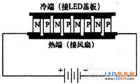
A thermoelectric cooler is a semiconductor device whose PN junction is composed of two different conductive materials, one carrying a positive charge and the other carrying a negative charge. When a current passes through a junction, the two charges leave the junction region and simultaneously There is heat to achieve the purpose of cooling, and its working principle is shown in the figure below.

Compared with other high-power LED heat dissipation structures, the thermoelectric refrigeration structure has the advantages of energy saving, small size, and easy integration with the LED module . At present, some scholars at home and abroad have conducted research on the application of thermoelectric refrigeration structures on high-power LED modules. Tian Dalei et al. applied the thermoelectric refrigeration structure to the heat dissipation system of the LED, and studied the cooling condition of the LED and the thermoelectric cooler under different currents through experimental tests, and measured the junction temperature of the LED. The results show that the thermoelectric refrigeration structure is adopted. The high-power LED display module can greatly reduce the operating temperature of the device. Compared with the structure, the substrate temperature can be reduced by more than 36%. This data shows that it is very good to use the thermoelectric refrigeration structure on the high-power LE D module. Cooling method.
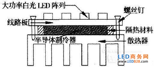
The field and others conducted a heat dissipation simulation on a 50W high-power LED module system using a thermoelectric refrigeration structure. The structure of the LED module system is shown in the following figure. The results show that the LED module system using thermoelectric cooling can make the LED junction to some extent. The temperature is reduced and the use of multi-stage semiconductor refrigeration for heat dissipation of high-power LED modules has broader research value.

Packaging material
It can be seen from the above analysis that the interface thermal resistance has a great influence on the total thermal resistance of the high-power LED. The main point of reducing the total thermal resistance of the LED is how to reduce the interface thermal resistance. Therefore, it is very important to select the appropriate thermal interface material and substrate material.
Thermal interface material
At present, the thermal interface materials commonly used in LED packaging are thermal conductive adhesives, conductive silver adhesives, and the like.
(a) Thermal adhesive
The main component of the commonly used thermal adhesive is epoxy resin, so its thermal conductivity is small, thermal conductivity is poor, and thermal resistance is large. In order to improve its thermal conductivity, a high thermal conductivity material such as aluminum oxide, boron nitride, silicon carbide or the like is usually filled inside the substrate. The thermal conductive adhesive has the advantages of insulation, heat conduction, shockproof, convenient installation, simple process, etc., but its thermal conductivity is very low (generally lower than 1w/mk), so it can only be applied to LED packaging devices that do not require high heat dissipation.
(b) Conductive silver glue
The conductive silver paste is a GeAs, SiC conductive substrate LED, a red, yellow, yellow-green chip LED package with a back electrode, or a key packaging material in the glue preparation process, having a fixed bonding chip, conductive and heat conduction, and transmission. The role of heat has an important influence on the heat dissipation, light reflectivity, and VF characteristics of the LED device . As a thermal interface material, conductive silver paste is widely used in the LED industry . At the same time, some scholars have conducted research on the application of conductive silver paste in LED. Hao Xiaoguang obtained the single-component solvent-free room temperature storage heat-dissipation type conductive silver paste from the conductive mechanism of conductive silver glue, the performance index of high-reliability conductive silver glue for LED package, and the testing technology. Has a good prospect.
Substrate material
Through the above analysis, a certain heat dissipation path of the LED package device is from the LED chip to the bonding layer to the internal heat sink to the heat sink substrate and finally to the external environment. It can be seen that the heat dissipation substrate is important for the heat dissipation of the LED package, and thus the heat dissipation substrate must be It has the following characteristics: high thermal conductivity, insulation, stability, flatness and high strength.
(a) MCPCB
The metal-based printed board (MCPCB) is bonded to the metal with high thermal conductivity (copper, aluminum, etc.) on the original printed circuit board to improve the heat dissipation effect of the electronic device. MCPCB is the key link connecting the internal and external heat dissipation paths. It has the following functions: 1 heat dissipation channel of LED chip; 2 electrical connection of LED chip; physical support of 3 LED chip.
The advantage of MCPCB is that it is relatively low cost and can be mass-produced, but it also has certain disadvantages: 1 The thermal conductivity is low, and the thermal conductivity of MCPCB can reach 1-2.2 W/(m·K). The thickness of the insulating layer in the 2MCPCB structure should be moderate, neither too thick nor too thin. Too thick insulation layer increases the thermal resistance of the entire MCPCB to affect the heat dissipation effect; the insulation layer is too thin, if the voltage applied to the MCPCB is too high, it will break through the insulation layer, resulting in a short circuit. In order to improve the thermal conductivity of MCPCB, Li Huaping optimized the process parameters of 20um to 40um plasma micro-arc oxidation (MAO) membrane through a series of experiments, and the thermal conductivity reached 2.3 W/(m·K). The thermal resistance of MAO-MCPCB substrates is lower (less than 10K/W), making this type of heat-dissipating substrate a big hit in the LED industry and even the general lighting industry.
(b) Ceramic substrate
The ceramic sintered substrate has good heat dissipation, high temperature resistance, moisture resistance, breakdown voltage, and breakdown voltage, and has good thermal expansion coefficient matching, and has the characteristics of reducing thermal stress and thermal deformation. Therefore, ceramics are expected to become an important substrate material in high-power LED packaging in the future. At present, the most commonly used ceramic materials are alumina, aluminum nitride, cerium oxide, silicon carbide, and the like. The properties of these commonly used ceramic materials are shown in the table below.

The data of the table shows that the three materials of aluminum nitride, cerium oxide and silicon carbide have better thermal conductivity, and the thermal conductivity of alumina is relatively poor, about one-seventh of that of aluminum nitride. However, among the three materials with high thermal conductivity, BeO is toxic. If it is inadvertently sucked into the lungs, it will cause pulmonary rickets. At present, some countries in the world have begun to ban the material; although AlN has high thermal conductivity, The technical threshold is relatively high, so the price is relatively high; pure SiC is not completely insulated, it is necessary to add a small amount of BeO and other materials to make it completely insulated, and the sintered SiC has a relatively high dielectric constant, which is not suitable for doing. Substrate material; in addition to poor thermal conductivity, Al2O3 has higher cost, but it has the advantages of good mechanical properties, mature production process and low cost. Therefore, in the future research and development and production work, in order to select a suitable ceramic material as the substrate material, the properties and cost of the four materials should be comprehensively considered.
Conclusion
Through the analysis of the thermal resistance of high-power LED devices, and the specific discussion from the two aspects of package structure and packaging materials, the following conclusions are drawn:
1) In high-power LED package devices, to achieve low thermal resistance and fast heat dissipation, package structure has become a key technology. It is a hot topic in the future to find a better package structure to improve the heat dissipation of LED package devices.
2) To solve the heat dissipation problem of high-power LED package devices, it is necessary to select suitable packaging materials (including thermal interface materials and substrate materials, etc.). In the process of selecting the thermal interface material and the substrate material, the appropriate material should be selected according to the appropriate occasion. The common thermal interface material used in general high-power LED packages is conductive silver paste, and the more common substrate is ceramic substrate.
Barrier Terminal Block
Terminal blocks are used to facilitate the connection of wires. In fact, they are a piece of metal sheet sealed in insulating plastic. There are holes at both ends to insert wires and screws to fasten or loosen them. For example, two wires sometimes need to be connected and sometimes need to be disconnected. At this time, they can be connected with terminals and can be disconnected at any time without having to connect them It's very convenient and fast to weld or wind together. And it is suitable for a large number of wire interconnection. In the power industry, there are special terminal blocks, terminal boxes, all of which are terminal blocks, single-layer, double-layer, current, voltage, common, breakable, etc. A certain crimping area is to ensure reliable contact and enough current.
Barrier Terminal Block
ShenZhen Antenk Electronics Co,Ltd , https://www.pcbsocket.com