Using SCM software to simulate the operation method of spi interface
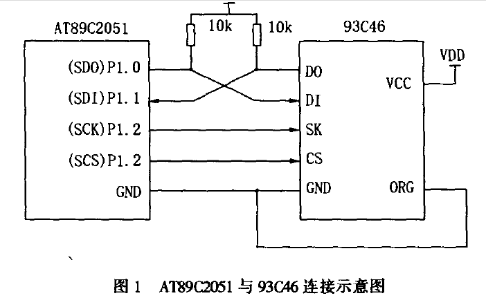
SPI (Serial Peripheral Interfacer) is a synchronous serial communication interface introduced by Motorola. It is used in the serial connection between the microprocessor controller and the peripheral expansion chip. Standards, at present, various semiconductor companies have introduced a large number of chips with various functions, such as RAM, EEPROM, FlashROM, A/D converter, D/A converter, LED/LED display driver, with SPI interface. I/O interface chips, real-time clocks, UART transceivers, etc., provide extremely flexible and inexpensive options for user peripheral expansion. Since the SPI bus interface only occupies four I/O lines of the microprocessor, the SPI bus interface can simplify the circuit, save many interface devices and I/O lines in the conventional circuit, and improve the reliability of the design. Taking AT89C205l MCU analog SPI bus operation serial EEPROM 93CA6 as an example, as shown in Figure 1, the implementation method of simulating SPI bus through software using I/O port of MCU is introduced. Here, only the timing of the read command and the application subroutine are introduced.

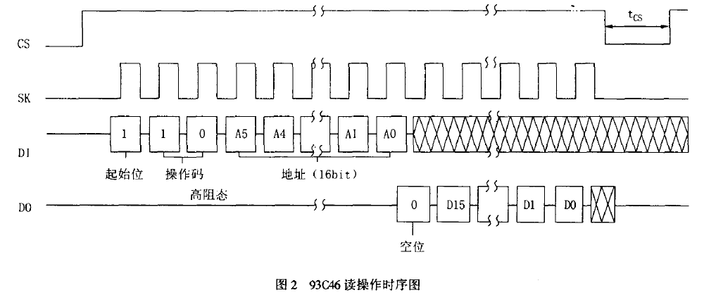
As a slave device, the 93CA6 uses four I/O lines: the serial clock line (SK), the output data line DO, the input data line DI, and the active-high slave select line CS. The data transmission format is high (MSB) first and low (LsB). The timing of the read command of the 93C46 SPI bus interface is shown in Figure 2.

Software simulation SPI interface implementation method
For the AT89C2051 microcontroller without the SPI serial bus interface, software can be used to simulate the operation of the SPI. Figure 1 shows the hardware connection diagram of the AT89C2051 microcontroller and the serial EEPROM 93C46. Among them, the P1.0 simulates the SPI master device. Data output SDO, P1.2 analog SPI clock output SCK, P1.3 analog SPI slave select SCS, P1.1 analog SPI data input SDI.
After the power-on reset, first set the initial state of P1.2 (SCK) to 0 (idle state). Read operation: AT89C2051 first sends a 1-bit start bit (1), a 2-bit opcode (10), a 6-bit read data address (A5A4A3A2A1A0) through the P1.0 port, and then reads a 1-bit vacancy through the P1.1 port ( 0), then read the l6 bit data (high position first). Write operation: AT89C2051 first sends a 1-bit start bit (1), a 2-bit operation code (01), a 6-bit written data address (A5A4A3A2A1A0) through the P1.0 port, and then sends the written l6 through the P1.0 port. Bit data (high order first), a write enable command is sent before the write operation, and a write disable command is sent after the write. Write enable operation (WEN): The write operation first sends a 1-bit start bit (1), a 2-bit opcode (00), and 6-bit data (11XXXX).
Write disable operation (WDS): The write operation first sends a 1-bit start bit (1), a 2-bit opcode (00), and 6-bit data (00XXXX).
The following describes the subroutine for simulating SPI with C51.
/ / First define the I / O port
Sbit SDO=P1^0;
Sbit SDI=P1^1;
Sbit SCK=P1^ 2;
Sbit SCS=P1^3;
Sbit ACC_7= ACC^7;
Unsigned int SpiRead(unsigned char add)
{
Unsigned char i;
Unsigned int datal6;
Add&=0x3f;/*6-bit address*/
Add |=0x80;/*Read opcode l0*/
SDO=1; /* send 1 as the start bit*/
SCK=0;
SCK=1;
For(i=0;<8;i++)/*Send opcode and address*/
{
If(add&0x80==1)
SDO=1;
Else
SDO=0;
SCK=0; /* Receive data from the rising edge of the device*/
SCK=1;
Add<<= 1;
}
SCK=1; /* sends data from the falling edge of the device clock line, and reads 1 bit of data*/
SCK=0;
Datal6<<= 1;/*Read 16-bit data*/
For(i=0;<16;i++)
{
SCK= 1;
_nop_();
If(SDI==1)
Datal6|=0x01;
SCK =0;
Datal6< < =1;
}
Return datal6;
}
For different serial interface peripheral chips, their clock timing is different. The above subroutine is for a device that inputs (receives) data on the rising edge of SCK and outputs (transmits) data on the falling edge. These subroutines are also applicable to other serial peripheral interface chips that are output on the rising and falling edges of the rising edge of the serial clock. As long as the output level of P1.2 (SCK) is changed in the program, the corresponding adjustment can be made. .
Our company specializes in the production and sales of all kinds of terminals, copper terminals, nose wire ears, cold pressed terminals, copper joints, but also according to customer requirements for customization and production, our raw materials are produced and sold by ourselves, we have their own raw materials processing plant, high purity T2 copper, quality and quantity, come to me to order it!
Copper Connecting Terminals,Cable Lugs Insulated Cord End Terminals,Pvc Insulated Cord End Terminal,Cable Connector Insulated Cord End Terminal
Taixing Longyi Terminals Co.,Ltd. , https://www.lycopperterminals.com