How to solve the power density problem
Author: ON Semiconductor Marketing Manager Jennifer Joseph
Integration is the foundation of solid-state electronics, and the ability to bring together similar and complementary functions into a single device drives the entire industry. With the development of packaging, wafer processing, and lithography technologies, functional density continues to increase, providing higher energy efficiency solutions in both physical size and power.
For product developers, power density is a constant challenge. The demand for higher currents at various voltages (usually well below the system bus) brings the need for smaller buck regulators. The regulator can reduce the voltage from up to 48 V to 1 V through multiple amplifiers in a single pole, allowing it to be close to the load point and still provide more than 95 percent of efficiency.
The combination of a high level of integration and power conversion is not a traditional good match, because generally, the processes used by both are not fully compatible. In some cases, unavoidable compromises can be tolerated, such as providing a lower power level DC/DC regulator over a relatively narrow input voltage range, or a negligible case of low power efficiency. Unfortunately, such compromises are becoming more and more intolerable to system developers.
A few power regulators now provide a good level of integration, but they are generally poor in performance and energy efficiency. For more and more applications that cannot be compromised in this regard, this often means that the level of integration may be limited by the controller and low/high-end drivers for the external MOSFETs. However, the ideal solution would be to integrate all the buck converter functions into a single, small, and energy-efficient device that combines controllers, drivers, and MOSFETs to provide a stronger overall system advantage.
Integrated power
There are many reasons for integration. In digital or mixed-signal solutions such as microcontrollers, integration allows common functions in a series of applications to be merged together. Putting them together in a single device creates a solution that, while attracting a significant number of manufacturers, often also reduces overall BoM costs. In this case, the advancement of the semiconductor manufacturing process adopted has enabled integration.
In power devices, integration can also provide cost advantages in a more efficient way. For example, tighter integration between the major components used for the step-down conversion can provide direct energy efficiency gains, which not only means lower BoM costs but also can save system energy consumption. In general, manufacturers can also achieve lower overall system cooling requirements due to improved energy efficiency. This can directly save the total cost of ownership in more and more applications, such as telecommunications and network equipment, base stations, industrial automation (including robots), household appliances and power tools, vending machines, games and financial machines (such as ATM (machines), and power supplies used to charge portable devices.
Multi-chip module
Single chip or multi-chip modules can be used to focus multiple components in a single package. The advantage of a multi-chip module is that it can avoid the large amount of compromise involved in the monolithic process in terms of the components that can be integrated. For component manufacturers such as ON Semiconductor, having the most suitable technology can provide an optimized method for developing multi-chip modules.
At a higher level, a synchronous buck regulator topology has three key functions, namely, controllers, gate drivers, and switching power MOSFETs. There are devices that can successfully integrate controllers and drivers for use with external MOSFETs, but seldom integrate all three functions into a single device, giving system engineers real advantages.
The FAN650xx family of voltage-mode synchronous buck regulators provides this level of integration. Targeted integration means that each element is designed and optimized for this task, resulting in a multi-chip module that combines class-leading current output with performance levels that cannot be achieved using discrete components.
The family currently includes three devices with different current outputs, 6A, 8A, or 10A, respectively. All devices maintain pin compatibility and are available in a space-saving 6 mm x 6 mm PQFN package, which means that even after the PCB design is complete OEMs can also select the most suitable device for their application. Figure 1 shows a functional diagram of the FAN650xx in a typical application.
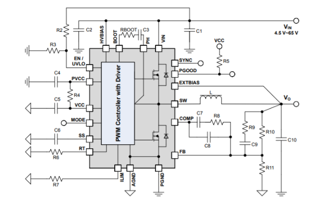
Figure 1: FAN650xx in a Typical Application
One of the main advantages of integrating high-side and low-side MOSFETs in the same package is that it can be optimized by the driver. In the traditional solution, the MOSFET is external and selects according to the output current requirement. Although this may be helpful, it does present some challenges when designing for demand currents.
Although the actual supply current that can be provided is still limited by the integrated gate driver capacity, the main challenge of the external MOSFET is to close the control loop based on sensing the high-side current. This is a key part of the overall solution because it provides voltage regulation and overcurrent protection. The integration of the internal MOSFET with the controller and driver design means that the temperature coefficient between the various parts of the circuit is matched more closely, providing higher accuracy. The topology with an external MOSFET does not have this close match, resulting in reduced energy efficiency.
Another advantage of actually developing components for multichip solutions is the ability to achieve tighter design optimization between gate drivers and MOSFETs. This means that the slew rate of the driver can be adjusted according to the MOSFET (here, ON Semiconductor's PowerTrench MOSFET technology is used). This can provide a lower ringing of the switch node and there is no risk of breakdown or cross conduction. Because the modular approach means that the current power supply design can only have one single point of failure, reliability is also improved.
Multi-mode operation
In addition to the advantages of high integration (including better thermal performance) (see below), the FAN650xx series offers multiple modes of operation for higher design flexibility. This includes CCM and DCM in main mode and non-primary mode. The mode pins on the device control whether it can operate in pulse modulation or frequency synchronization mode, which brings many design possibilities. Figure 2 AC shows a typical application example for the FAN650xx series.
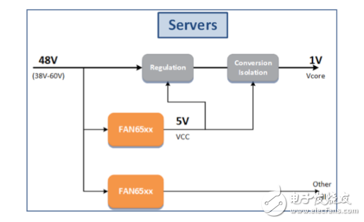
Figure 2A
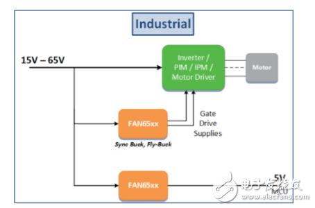
Figure 2B
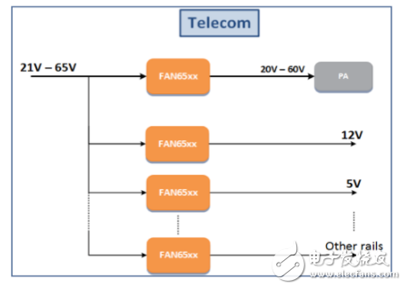
Figure 2C
Figure 2D
Figure 2 AD is a design example of how the FAN650xx family works in forced CCM or DCM mode. In the forced CCM mode, it maintains a continuous conduction mode regardless of load conditions, and the frequency is constant, enabling low ripple output. If the device operates in DCM mode, pulse skipping occurs at light loads, but when the inductor current is higher than 0A, it automatically switches to CCM mode, which in turn provides higher operating efficiency for light-load or standby applications.
When in the main mode of the frequency synchronization mode, the device generates a clock signal that is 180° out of phase with its own clock, allowing multiple devices to synchronize while maintaining minimum input ripple, which in turn improves the overall system efficiency.
Thermal management
The multi-chip module design means that the source of the low-side MOSFET can be physically connected to a large ground plane. This in turn uses perforations to create an efficient thermal path for the inner layer of the PCB. This design improves the thermal characteristics of the module and further increases overall energy efficiency.
The PowerNone® MOSFET and the thermally enhanced, 6 x 6 mm PQFN package enable the FAN6500xx series to provide high power density performance.
In Figure 3, the FAN65004B is used to build a converter from 48V input to 28V output at 5A output current.
• The case temperature thermocouple is on the high-side FET.
• T1 = 117.90C
• The ambient temperature thermocouple is located at the bottom of the circuit board.
• T2(Ta) = 98.90C
The program can provide 140 W of output power with 97% efficiency, and the temperature rises only 19 ÌŠC.
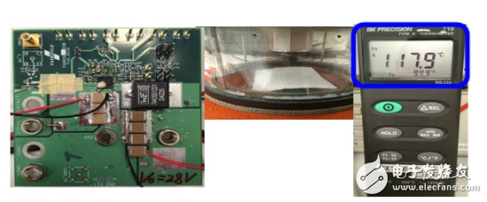
Figure 3: Example Thermal Energy Efficiency for FAN650xx Series
The FAN650xx series of voltage-mode synchronous buck regulators provide a complete solution in a single module, helping system engineers and power supply designers achieve higher power densities for a wide range of applications. With a wide input voltage range of 4.5 V to 65 V and output voltages from 0.6 V to 55 V and continuous currents from 6 A to 10 A, pin-compatible products in this family take power density and integration to new levels.
Suizhou simi intelligent technology development co., LTD , https://www.msmvape.com