Dual Gigabit Network Interface Design for Eight-Core Floating-Point DSP
Gigabit network interface has the advantages of fast data transmission rate, convenient connection and plug and play, which makes it widely used. With the development of electronic technology and processors, the data communication rate of many applications exceeds the actual transmission rate of the Gigabit Ethernet port. For example, in A/D sampling, it is necessary to directly store the sampled data of the A/D conversion. If the A/D conversion bit number is 16 bits and operates at 100 MHz, the actual data amount is 1.6 Gbps. In order to achieve high-speed transmission, a higher transmission rate interface, such as PCIe or RapidIO interface, must be used. However, these interfaces do not have a plug-and-play function, and they cannot be directly connected to many industrial existing devices, which limits their applications.
DSP (Digital Signal Processor) has a high operating frequency, and its internal integrated hardware network MAC interface, external one physical layer chip can easily realize Gigabit network communication. Multi-core DSP chips can be connected to multiple Gigabit Ethernet ports, making them suitable for high-speed data transmission applications. This paper introduces an embedded dual Gigabit network interface based on multi-core digital signal processor TMS320C6678, which realizes a single chip to connect two Gigabit Ethernet ports. These two network ports can transmit data independently or jointly, and improve data transmission. Actual data transfer rate.
1. C6678 and its structure
The TMS320C6678 is an 8-core floating-point DSP from TI's multi-core processors. Each core can operate up to 1.25GHz. Each core can provide 40GMAC fixed-point calculation or 20GFLOP floating-point computing capability. A single chip can provide 320GMAC or 160GFLOP computing power. The on-chip structure of the TMS320C6678 is shown in Figure 1.
Each core of the TMS320C6678 has a 32KB program, 32KB of data, and 512KB of Level 2 Cache memory. The chip has a 4MB shared SRAM. The TMS320C6678 has a DDR3 controller interface that can be connected to DDR3 with a direct addressing range of 8GB. The TMS320C6678 has internal and external interfaces such as RapidIO, PCIe, EMIF, SPI, and I2C bus. These interfaces interact with each processor through the on-chip high-speed interconnect bus.
The network-related on-chip devices are shown in the gray module in the lower right corner of Figure 1. They mainly include two external SGMII interfaces, Ethernet switching and network switching modules, and security accelerators and packet accelerators for data management, which can quickly detect data. Verification and whether the protocol complies with the network standard, and discards the wrong data directly, reducing the burden on the CPU. In order to speed up the data exchange between the network and the CPU, the on-chip queue manager is used to manage functions such as caching and distribution of network packets or network frames. These data are read and written using packet DMA and do not require CPU involvement.
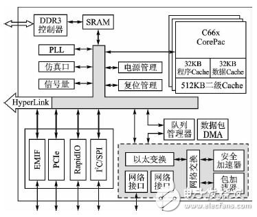
Figure 1 TMS320C6678 internal structure diagram
Other on-chip devices in the TMS320C6678 include PLLs, emulation ports, semaphores, power management, and reset management. The PLL configures the working clock of the CPU and peripherals; the emulation port is used to connect the emulator to realize the monitoring of the software operation; the semaphore realizes the control of the semaphore in the DSP/BIOS operating system; the power management realizes the control of the current and voltage of the whole chip. ; reset management configuration startup mode, hard reset for full boot, soft reset for partial boot.
2. 88E1111 and its structure
There are many network physical layer chips, and they are generally compatible with one or more interface standards such as MII, RMII, and SGMII. However, the TMS320C6678 only provides the SGMII interface, so the physical layer chip connected to the TMS320C6678 must have the SGMII interface. This article uses two Marvell 88E1111 physical layer chips for dual Gigabit network connectivity. The on-chip structure of the 88E1111 is shown in Figure 2.
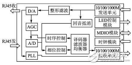
Figure 2 Internal structure of 88E1111
The analog signal with modulated data sent from the network RJ45 interface is converted into a digital signal by A/D conversion, and then subjected to equalization, shaping filtering and decoding, and then transmitted by the receiving unit to the MAC chip to realize data reception. The data sent by the MAC is shaped and filtered, and then converted into an analog signal by D/A and sent to the RJ45 interface. In order to reduce the bit error rate, the 88E1111 has internal phase-locked loop (PLL), automatic gain control (AGC), timing/phase control, echo cancellation and other modules. These modules are designed to improve the reliability of data transmission in different environments or different environments. Under external devices, high-speed and reliable communication is possible. The LED control module in Figure 2 implements the light display during data transmission, the MDIO module implements link establishment and status monitoring, and the clock module provides the working clock.
3. Hardware design
The hardware design mainly includes TMS320C6678 and two 88E1111 interfaces, 88E1111 and RJ45 interfaces, and 88E1111 hardware configuration design.
The network module structure of TMS320C6678 is shown in Figure 3. An on-chip integrated 3-port Ethernet switch is responsible for exchanging data between two Gigabit Ethernet ports to the host, and providing switching interrupts to the host. The host can receive and send data in real time through interrupts. The host configures or monitors the external physical layer chip through the bus, and the configuration and monitoring data is connected to the physical layer chip through the MDIO interface.
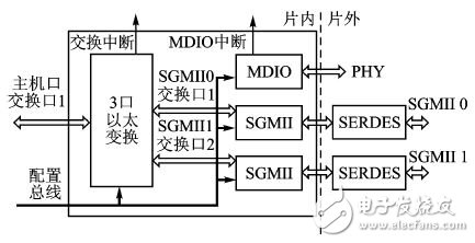
Figure 3 TMS320C6678 network module structure
Figure 4 TMS320C6678 and 88E1111 interface TMS320C6678 and two 88E1111 interface circuit shown in Figure 4. The TMS320C6678 adopts the SGMII (Serial Gigabit Media Independent Interface) interface and is compatible with 10/100/1000M working mode. SGMII is a serial data transceiver with fewer pin connections. As can be seen from Figure 4, there are actually only two pairs of differential lines that are transceived and connected to the corresponding 88E1111 pins. The read and write clocks are implicitly transmitted on the data and are automatically identified by the hardware without software involvement.
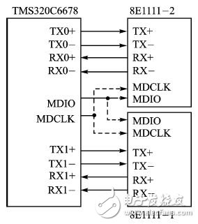
Figure 4 Interface of TMS320C6678 and 88E1111
MDIO and MDCLK are the data and clock of the internal MDIO module of TMS320C6678. It is used to establish connection between TMS320C6678 and 88E1111. The TMS320C6678 can configure 88E1111 through this interface or read the information of 88E1111. Since the interface level of the MDIO module of the 88E1111 is 2.5V, and the interface level of the MDIO module of the TMS320C6678 is 1.8V, the voltage conversion chip needs to be added between the two. This design uses PCA9306 to realize voltage conversion. The interface circuit is shown in Figure 5. Show.
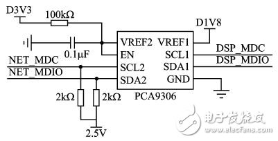
Figure 5 voltage conversion circuit of MDIO interface
It should be noted that because there are two 88E111 chips, MDIO and MDCLK pins are directly connected to two chips, MDIO can control up to 32 physical layer chips, and the physical layer chip addresses are respectively 1~32.88E1111. 6 is shown.
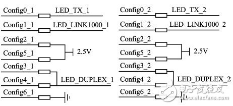
Figure 6 Hardware configuration of 88E1111
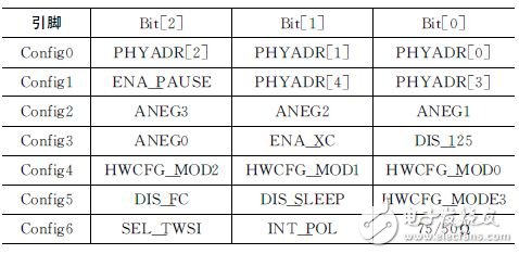
Table 1 shows the corresponding configuration information. According to Figure 6 and Table 1, it can be seen that the addresses of 88E111 are 4 and 8, respectively.
Table 1 Configuration Pin Settings
4. Software design
System software design includes hardware initialization, network configuration, and data communication flow. The workflow after reset of TMS320C6678 is shown in Figure 7. Configure the first network port first, and record the status and configure the second network port. As long as the configuration of the two network ports is successful, the EMAC module of the TMS320C6678 is configured to set up the sending and receiving buffers and send and receive tasks for the successfully configured network ports. After these configurations are completed, data transmission and reception of the network can be realized. It should be noted that in the user application, it is necessary to consider the failure of the network port configuration. For example, a user application transmits 1.2 Gbps of data in real time through a dual network port. If a network port fails to be configured, the application should have a mechanism to reduce the real-time transmission rate to less than 0.8 Gbps. The actual transmission rate of a single network port may be lower. 0.8Gbps). In this paper, the hardware system can transmit 1.5Gbps data without any other task overhead (no error is considered during transmission, no retransmission is performed).
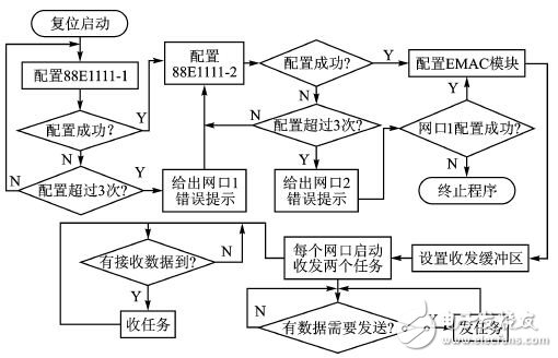
Figure 7 data communication process
Conclusion
Communication interfaces exceeding 1 Gbps transmission rate generally adopt optical fiber, PCE, PCIe and other interface modes. In this paper, the dual network port method can reduce the equipment requirements and facilitate the connection with existing equipment. The use of multi-core DSP to improve the processor's working ability, in the process of ensuring large-capacity data transmission, the processor still has the ability to calculate data. The dual network port design solution can make up for the insufficient transmission rate of the single network port and reduce the hardware complexity of other interfaces, which is a useful supplement between the two. It has certain application value in embedded devices.
Wall Mounted Battery,Wall-Mounted Lithium-Ion Battery,Residential Wall-Mount Battery,Wall Mounted Lithium Battery
JIANGMEN RONDA LITHIUM BATTERY CO., LTD. , https://www.ronda-battery.com