Broadband video switching integrated circuit AD8108/AD8109 and its application
Abstract: This paper introduces the main functions, working principle and programming logic of AD8108, AD8109, and points out several problems that should be paid attention to when designing the software and hardware of 8×16 video switching system with AD8108. Practice shows that the switching system has good reliability and strong anti-interference ability.
Keywords: AD8108, AD8109; video switching matrix; broadband video
This article refers to the address: http://
0 Introduction Video matrix switchers are mainly used in the field of television video. With the development of computer technology and multimedia technology, its application range is more and more extensive. Based on this, many large companies have launched broadband video switching ICs. Among them, the AD8108/AD8109 produced by American Analog Devices not only integrates the functions realized by many discrete components, but also has low cost, long service life, good electromagnetic compatibility and good expandability. This paper starts with the function of the wideband video switching integrated circuit AD8108/AD8109, focuses on its working principle and control logic and programming, and discusses the problems that should be paid attention to when applying the application of AD8108.
1 Functional Principle of the AD8108/AD8109 The AD8108/AD8109 is a high-speed 8×8 video switching matrix with a -3 dB bandwidth greater than 250 MHz, a channel switching time of less than 25 ns, and a loss of less than 1%. The AD8108/AD8109 have only -83 dB crosstalk and -98dB isolation at 5 MHz, with a differential gain error/differential phase error of better than 0.02%, 0.02°. The AD8108/AD8109 are ideal for video signal switching due to their 0.1 dB gain flatness.
1.1 Pin Function The AD8108/AD8109 are available in a TQFP package and have a total of 80 pins. The pin structure is shown in Figure 1. The functions of each main pin are as follows:

INxx: analog input channel, xx indicates channel number 00~07;
DATA IN: Serial data input, compatible with TTL level;
CLK: clock, falling edge valid, compatible with TTL level;
DATA OUT: Serial data output, compatible with TTL level;
: Data control terminal. When low, the register data is allowed to be sent directly to the switch matrix; when high, the data is latched;
: chip enable terminal, active low;
: reset terminal, active low;
: Work mode selection end. Low level, select serial mode: When high level, select parallel mode.
OUTyy: analog output, yy indicates channel number 00~07;
A2~A0: Parallel data input terminal, compatible with TTL level,
Where A0 is the lowest position;
D2~D0: Parallel data input terminal, compatible with TTL level,
Where D0 is the lowest bit;
D3: Parallel data input and output enable, compatible with TTL.
NC: Suspended end.
Others such as analog ground (AGND), digital ground (DGND), analog negative power supply (AVEE), analog positive power supply (AVCC), etc. are relatively easy to understand, so I will not repeat them here.
1.2 Principle of Operation AD8108 (G=1) and AD8109 (G=2) have the same core. Its capacity is 8 × 8. It is mainly composed of a 32-bit shift register, a parallel latch, a decoder, a 64-point switching matrix, and an output buffer. FIG. 2 is a block diagram of its internal structure.

As can be seen from Figure 2, the AD8108/AD8109 have two control modes, which are controlled by the 32-bit shift register in the chip to switch between 8 inputs and 8 outputs.
When low, select serial mode. In this mode, the output ports are determined in the default order without entering an address. The AD8108/AD8109 have eight output ports, which correspond to 4-bit data, that is, D3 to DO. D3 is used to block or enable the output port. When D3 is 0, D2~DO is invalid, and the corresponding output port is blocked. D2~DO are used to determine the input port connected to an output port. DATA IN is driven by the falling edge of the CLK signal, and sequentially transmits OUT7[D3], OUT7[D2], OUT7[D1], OUT7[D0], ..., OUT0[D3], OUT0[D2], OUT0[Dl], The OUT0[D0] data is transferred to the 32-bit shift register in the chip, and the shift register controls the corresponding switching relationship between the input signal and the output signal. When all 32-bit data is input, the CLK signal is stopped and becomes a low level, and the input and output of the matrix are switched according to the 32-bit data just input. If the CLK signal is not stopped, the switching matrix data is dynamically changed. When it goes high, the 32-bit data is latched. The use of serial mode is characterized by the use of fewer control signals, but at a slower speed: each time the input and output configuration is changed, 32 bits of serial data must be provided in order to change the entire matrix data: in addition, the serial data output It is also convenient to build a large-capacity matrix switcher. In this case, you only need to connect the DATA OUT end of one chip to the DATA IN of another chip, while others (such as CLK, , and ) should be connected in parallel.
When it is high. Select the parallel mode. In this mode, when low, set high and on the falling edge of CLK, the logic values ​​on the pins including A2~A0, D3~DO will enter with 4 bit parallel loading. Function in the 32-bit shift register. As for which 4-bit unit of the 4-bit data D3 to D0 is loaded into the 32-bit shift register, it is determined by A2 to A0. A2~A0 divides the 32-bit shift register into eight 4-bit unit segments, and each 4-bit unit segment corresponds to one output buffer. When it is low level, the content of the above shift register enters the parallel latch module, and after 8x4:8 decoding, the switch matrix can be controlled to realize 8 inputs by D3, D2~D0, A2~A0. Any of the inputs is output to any of the eight outputs. The characteristics of the parallel mode: First, the use of many control signals, but the speed is fast; Second, when changing the working mode of a single output channel, there is no need to reprogram the entire switching matrix.
2 Timing and Control Logic Programming The signal channel bandwidth of the AD8108/AD8109 is not less than 250MHz (-3dB), which is higher than the bandwidth of computer video signals and many radar video pulses, so it can be used in many widebands such as composite video, component video, and compressed video. Signal switching; the chip integrates the output buffer in the chip, reducing parasitic capacitance and making it more resistant to interference; this high-density integrated module makes it easier to integrate larger-scale video matrix switching circuits; The serial or parallel control mode has simple control and strong driving capability, and can drive 150Ω load. In addition, the chip's low power consumption, operating current is only 45 mA, and has an output disable function that allows the outputs of multiple chips to be directly connected.
2.1 Timing Diagram The serial mode timing diagram of the AD8108/AD8109 is shown in Figure 3. In the figure, both the clock signal CLK and the refresh signal are valid for the falling edge. In particular, the data setup time t1 is at least 20 ns, and the latch time t6 is at least 50 ns, that is, after the data is established, the serial output data is not longer than 180 ns (t7). Therefore, when a set of data (D3-D0) is transmitted, it can be valid immediately on the falling edge of the clock, (lowed to low level) to latch the data; the clock can also be stopped and validated every other time.

Figure 4 shows the timing diagram when it is operating in parallel mode. In this mode, the data setup time and the signal latch time are the same as the serial mode.
2.2 Programming of Control Logic Serial operation mode usually uses pins, CLK, DATA IN, and . The first step should be set low in the case of active low to operate in serial mode. In the second step, 32 bits of data are serially input to complete the change of the input and output configuration. Each output port corresponds to 4 bit bits (D3 ~ DO, D3 first input, if D3 is low level, the corresponding output is blocked, followed by D2 ~ D0 is meaningless), a total of 8 output ports, 8th The data of the output ports is input first; in the third step, when all the data of the 32 bits is input, the CLK signal is stopped, becomes a low level, and the input and output configuration of the matrix is ​​switched according to the 32 bit data just input. If it is low, the CLK signal does not stop. Then the switching matrix data is dynamically changed; in the fourth step, it becomes a high level, and the 32-bit data is latched.
Note that if multiple AD8108/AD8109 devices are cascaded, the number of bits required for a single change is the product of 32 and the number of devices. Serial data is first input to the DATA of the first chip
IN, then enter the other chips in turn, until the last chip. Therefore, the data given to the last chip is the front end of the programmed sequence.
The parallel mode of operation allows only one configuration of the output port to be changed at a time. Since one change takes only one CLK and cycle, the change speed is greatly improved. Parallel operation mode requires pins, CLK, D3-D0, A2 to A0, and . The first step is first set to high level in the case of active low, so that it works in parallel mode; the second step is set to high level, and set output address A2 ~ A0, and input address D2 ~DO, and the output enable terminal D3, so that the 4-bit data D3 to D0 are loaded into a 4-bit unit segment in the 32-bit shift register determined by A2 to A0. The third step is to set the low level. The data in the 32-bit shift register is latched into the parallel register, and the control matrix is ​​switched after 8x4:8 decoding.
It is important to consider that the reset signal cannot reset all registers in the AD8108/AD8109, except that all output channels of the switching matrix are disabled, and the switching logic in the registers is still placed in a random arrangement. Therefore, whether in serial mode or parallel mode, all shift registers must be programmed to the desired state after initial power-up.
3 AD8108/AD8109 Applications and Precautions The AD8108/AD8109 are high-density integrated modules that utilize the different features of their output enable and chip select enable to build large-size video switches that exceed 8x8. When building larger matrix switches, they can be used with the AD8116. Figure 5 shows an 8x16 video switching system using two AD8108s. The system can output any of the eight inputs to the 16 outputs, which can meet the radar direction detection function of a certain type of radar warning device. It is necessary to switch the narrow video sequence of two video channels to four channels and four channels for 16 channels.

The AD8108/AD8109 are primarily used for video switching. Due to the high frequency of the video signal and the wide frequency band, the following points should be noted when using the AD8108/AD8109:
(1) Signal channel bandwidth consideration Signal channel bandwidth is an important indicator of video switching system, which determines the technical difficulty, function and cost of video switching system. ADI's 8×8 matrix switching chip has AD8108/
The AD8109 has a -3 dB bandwidth of 325 MHz/250 MHz. Although these are much higher than the bandwidth of TV video signals and computer video signals, the channel bandwidth is often reduced after the entire system is designed. Experiments show that the former stage selects the AD8108 for small signal switching, the latter stage selects the AD8109 for switching and amplification, and pays attention to the impedance matching, which is beneficial to improve the channel bandwidth of the matrix switcher and strengthen the anti-interference ability of the system.
(2) Isolation requirements Isolation is an important indicator to measure the system's ability to resist crosstalk. Although the isolation of the AD8108/AD8109 is -83 dB/-75 dB at 5 MHz, the isolation is highly dependent on the frequency of the crosstalk signal. Therefore, after designing the entire system, the isolation index is often much lower. . Studies have shown that human eye vision is aware of a 3% difference in brightness, equivalent to -30 dB of isolation. The isolation of -45 dB is equivalent to 0.56% of noise (or crosstalk), well below 3%. Because there is enough margin, the human eye does not feel the crosstalk spot. Therefore, after designing the entire system, the isolation should be no less than -45 dB to meet the requirements.
(3) Large Switching Matrix Construction The biggest difference between the AD8108 and the AD8109 is the difference in gain. The gain of the AD8108 is +1, while the gain of the AD8109 is +2. Therefore, in the construction of large switching matrix, in order to reduce the crosstalk during switching, improve the signal channel bandwidth, and consider the strong driving capability of AD8109, AD8108 is generally used in the pre-stage, and AD8109 is used in the latter stage.
(4) Printed Board Design The AD8108/AD8109 are high-density integrated modules. The different features of output enable and chip select enable make them play an important role in building large switching matrices. In order to minimize the crosstalk generated by the system board, the grounding, shielding, signal path and power supply bypass must be carefully handled during the design. The specific attention should be paid to: First, the video signals are separated by thick ground lines; The analog ground and the digital ground should be strictly separated and connected only at the power supply; the third is that the analog power supply and the digital power supply are independent, and the power supply should be aligned with the direction of data transmission; the fourth is to use multi-point grounding shield, and the grounding wire should be as far as possible Thick, and configure decoupling capacitors in key parts; Fifth, when using multiple AD8108/AD8109 to form a large-capacity system, the control line and chip select line must be added with drive circuit.
(5) Software programming control When the software controls the switching, all the outputs should be disabled first, then the corresponding output is allowed, and then the corresponding input is turned on. Considering that the AD8108/AD8109 normally operate in parallel mode, the reset signal can only set all output channels of the switching matrix to disabled. It is not possible to reset all registers in the AD8108/AD8109, and the switching logic in the registers is still placed in a random arrangement. Therefore, after the initial power-on, both the and the disallowed are set low to prevent the matrix switch from being in an unknown state.
4 Conclusion Through the analysis and design of this paper, the 8x16 matrix switching system composed of two AD8108s has been successfully used in the test of the radar direction detection device of a certain type of radar warning device, and successfully realized the narrow pulse sequence in two channels of video. Switch to the four-way, four-band 16-channel switching function at different times. Practice shows that the switching system has high reliability and strong anti-interference ability.
Single Color Controller, also known as programmable lighting controller, the controller is the lighting program can be modified according to the needs of users, such as changing light flashing speed, time, synchronized, synchronous and asynchronous, and so on. And has good scalability and can be a combination of multiple control panels according to the needs of users synchronous and asynchronous operation to achieve higher requirements.
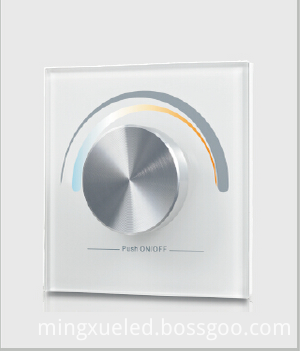
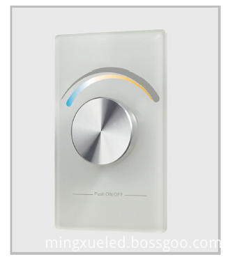
The Single Color Controller uses reliable hardware control 51 microcontroller core, and with the PC software editing lighting, download, and upgrade the computer USB interface communication, greatly improving ease of use controllers, but also energy-saving 60-70 %.
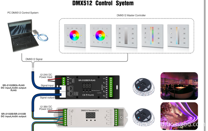
In supporting free software for easy editing, download programmed control program (ie, the light pattern), and has a unique software preview function, easy to modify, debug lighting effects . a Single Color Controller can make the eight output ports through the changing composition reached the end of the desired effect, Single Color Controller can also be a combination of a plurality of control panels to control more controllable way port (the largest currently available do 24 road extension technology will achieve more controllable way).
The control system can easily solve these problems is simple, low cost, but also more competitive. The controller software has now been three times to modify upgrades, making use of more convenient, more humane, we will better serve our customers.
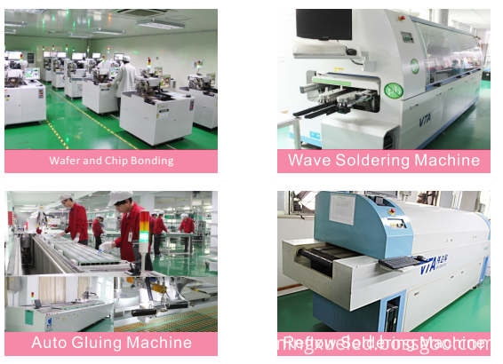
Mingxue Optoelectronics Co.,Ltd. has apply the I S O 9 0 0 1: 2 0 0 8 international quality management system certificate, For Single Color Controller, we apply the CE, RoHS and SAA certificate for our led lighting product.
Our R & D team can handle highly customized designs and offer OEM and ODM services.
We hope to set up a long-term partnership with you through our high quality products and our Sincere Service!

Single Color Controller
Single Color Controller,Single Color Rf Remote Control,Single Color Led Strip Controller,Mini Single Color Controller
Shenzhen Mingxue Optoelectronics CO.,Ltd , http://www.mingxueled.com